TECHNICAL ASSET FINGERPRINT
7f67d8ef65b2491f0e300b2d
Click to view fullscreen
Press ESC or click to close
FOUND IN PAPERS
EXPERT: gemini-2.0-flash VERSION 1
RUNTIME: nugit/gemini/gemini-2.0-flash
INTEL_VERIFIED
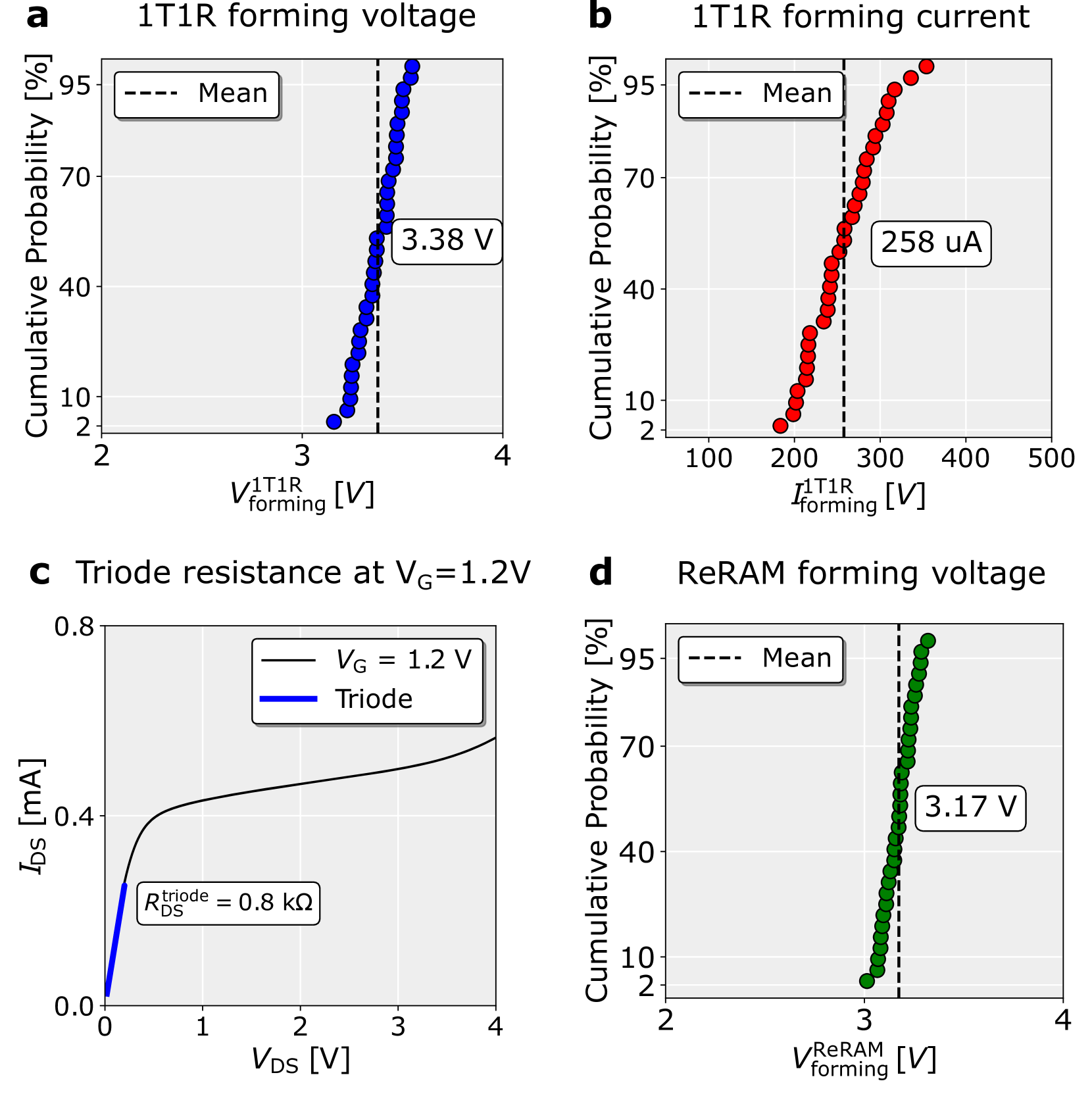
## Chart Compilation: Electrical Characteristics of 1T1R and ReRAM Devices
### Overview
The image presents four plots (a, b, c, d) illustrating the electrical characteristics of 1T1R (One Transistor One Resistor) and ReRAM (Resistive Random-Access Memory) devices. Plots a, b, and d show cumulative probability distributions for forming voltage and current, while plot c depicts the triode resistance at a specific gate voltage.
### Components/Axes
**Plot a: 1T1R forming voltage**
* **Title:** 1T1R forming voltage
* **X-axis:** V<sup>1T1R</sup><sub>forming</sub> [V] (1T1R Forming Voltage in Volts). Scale ranges from 2 to 4, with tick marks at every 1 unit.
* **Y-axis:** Cumulative Probability [%]. Scale ranges from 2 to 95, with tick marks at 10, 40, 70, and 95.
* **Data:** Blue dots represent the cumulative probability of the forming voltage.
* **Mean:** Dashed black vertical line indicating the mean forming voltage.
* **Annotation:** "Mean" in a rounded box at the top-left.
* **Value Label:** A rounded box indicates a voltage of 3.38 V.
**Plot b: 1T1R forming current**
* **Title:** 1T1R forming current
* **X-axis:** I<sup>1T1R</sup><sub>forming</sub> [uA] (1T1R Forming Current in microAmperes). Scale ranges from 100 to 500, with tick marks at every 100 units.
* **Y-axis:** Cumulative Probability [%]. Scale ranges from 2 to 95, with tick marks at 10, 40, 70, and 95.
* **Data:** Red dots represent the cumulative probability of the forming current.
* **Mean:** Dashed black vertical line indicating the mean forming current.
* **Annotation:** "Mean" in a rounded box at the top-left.
* **Value Label:** A rounded box indicates a current of 258 uA.
**Plot c: Triode resistance at V<sub>G</sub>=1.2V**
* **Title:** Triode resistance at V<sub>G</sub>=1.2V
* **X-axis:** V<sub>DS</sub> [V] (Drain-Source Voltage in Volts). Scale ranges from 0 to 4, with tick marks at every 1 unit.
* **Y-axis:** I<sub>DS</sub> [mA] (Drain-Source Current in milliAmperes). Scale ranges from 0.0 to 0.8, with tick marks at 0.0, 0.4, and 0.8.
* **Data:**
* Black line represents V<sub>G</sub> = 1.2 V.
* Blue line represents the Triode region.
* **Legend:** Located at the top-right, indicating the black line as "V<sub>G</sub> = 1.2 V" and the blue line as "Triode".
* **Annotation:** "R<sup>triode</sup><sub>DS</sub> = 0.8 kΩ" in a rounded box, indicating the triode resistance.
**Plot d: ReRAM forming voltage**
* **Title:** ReRAM forming voltage
* **X-axis:** V<sup>ReRAM</sup><sub>forming</sub> [V] (ReRAM Forming Voltage in Volts). Scale ranges from 2 to 4, with tick marks at every 1 unit.
* **Y-axis:** Cumulative Probability [%]. Scale ranges from 2 to 95, with tick marks at 10, 40, 70, and 95.
* **Data:** Green dots represent the cumulative probability of the forming voltage.
* **Mean:** Dashed black vertical line indicating the mean forming voltage.
* **Annotation:** "Mean" in a rounded box at the top-left.
* **Value Label:** A rounded box indicates a voltage of 3.17 V.
### Detailed Analysis
**Plot a: 1T1R forming voltage**
* The cumulative probability increases sharply between 3 V and 3.5 V.
* The mean forming voltage is approximately 3.38 V.
**Plot b: 1T1R forming current**
* The cumulative probability increases sharply between 200 uA and 300 uA.
* The mean forming current is approximately 258 uA.
**Plot c: Triode resistance at V<sub>G</sub>=1.2V**
* The blue line (Triode) shows a linear relationship between V<sub>DS</sub> and I<sub>DS</sub> up to approximately 0.5 V.
* The black line (V<sub>G</sub> = 1.2 V) shows a non-linear relationship, with the current increasing at a decreasing rate as V<sub>DS</sub> increases.
* The triode resistance is given as 0.8 kΩ.
**Plot d: ReRAM forming voltage**
* The cumulative probability increases sharply between 3 V and 3.2 V.
* The mean forming voltage is approximately 3.17 V.
### Key Observations
* The forming voltages for both 1T1R and ReRAM devices are clustered around 3 V, with 1T1R having a slightly higher mean forming voltage.
* The forming current for 1T1R devices is centered around 250 uA.
* The triode region of the transistor exhibits a linear I-V relationship, while the saturation region shows a non-linear behavior.
### Interpretation
The data suggests that the forming process for both 1T1R and ReRAM devices requires a specific voltage range to initiate the resistive switching. The relatively narrow distribution of forming voltages indicates a consistent and controlled fabrication process. The triode resistance plot provides insight into the transistor's behavior, showing the linear and non-linear regions of operation. The 1T1R device has a higher forming voltage and current compared to the ReRAM device, which could be attributed to differences in their material composition or device structure.
DECODING INTELLIGENCE...
EXPERT: gemma-3-27b-it-free VERSION 1
RUNTIME: google-free/gemma-3-27b-it
INTEL_VERIFIED
## Cumulative Distribution Plots & IV Curve: Device Forming Characteristics
### Overview
The image presents four separate plots characterizing the forming behavior of different resistive switching devices. Plots (a) and (d) show cumulative probability distributions of forming voltages for 1T1R and ReRAM devices, respectively. Plot (b) shows the cumulative probability distribution of forming current for 1T1R devices. Plot (c) displays an IV curve demonstrating the triode resistance of a device at a fixed gate voltage.
### Components/Axes
* **Plot a: 1T1R forming voltage**
* X-axis: V<sup>1T1R</sup><sub>forming</sub> [V] (Forming Voltage for 1T1R device) - Scale: 2 to 4 V
* Y-axis: Cumulative Probability [%] - Scale: 0 to 100%
* Data Series: Blue dots representing the cumulative distribution. Dashed black line representing the mean.
* **Plot b: 1T1R forming current**
* X-axis: I<sup>1T1R</sup><sub>forming</sub> [µA] (Forming Current for 1T1R device) - Scale: 100 to 500 µA
* Y-axis: Cumulative Probability [%] - Scale: 0 to 100%
* Data Series: Red dots representing the cumulative distribution. Dashed black line representing the mean.
* **Plot c: Triode resistance at V<sub>G</sub>=1.2V**
* X-axis: V<sub>DS</sub> [V] (Drain-Source Voltage) - Scale: 0 to 4 V
* Y-axis: I<sub>DS</sub> [mA] (Drain-Source Current) - Scale: 0 to 0.8 mA
* Data Series: Blue line representing the IV curve.
* **Plot d: ReRAM forming voltage**
* X-axis: V<sup>ReRAM</sup><sub>forming</sub> [V] (Forming Voltage for ReRAM device) - Scale: 2 to 4 V
* Y-axis: Cumulative Probability [%] - Scale: 0 to 100%
* Data Series: Green dots representing the cumulative distribution. Dashed black line representing the mean.
### Detailed Analysis or Content Details
* **Plot a: 1T1R forming voltage**
* The blue data points show a steep increase in cumulative probability between approximately 3.1 V and 3.5 V.
* The mean forming voltage is indicated by a dashed black line at approximately 3.38 V.
* **Plot b: 1T1R forming current**
* The red data points show a steep increase in cumulative probability between approximately 200 µA and 300 µA.
* The mean forming current is indicated by a dashed black line at approximately 258 µA.
* **Plot c: Triode resistance at V<sub>G</sub>=1.2V**
* The blue line shows a non-linear relationship between V<sub>DS</sub> and I<sub>DS</sub>.
* The current increases rapidly from 0 mA to approximately 0.4 mA as V<sub>DS</sub> increases from 0 V to 3 V.
* The triode resistance is labeled as approximately 0.8 kΩ.
* **Plot d: ReRAM forming voltage**
* The green data points show a steep increase in cumulative probability between approximately 3.0 V and 3.3 V.
* The mean forming voltage is indicated by a dashed black line at approximately 3.17 V.
### Key Observations
* The 1T1R devices exhibit forming voltages clustered around 3.38 V and forming currents clustered around 258 µA.
* The ReRAM devices exhibit forming voltages clustered around 3.17 V.
* The IV curve in plot (c) demonstrates a clear triode region with a resistance of 0.8 kΩ at V<sub>G</sub> = 1.2 V.
* All cumulative distribution plots show a relatively narrow distribution of forming voltages/currents, suggesting a consistent forming process.
### Interpretation
The data suggests that the 1T1R and ReRAM devices have different forming voltage requirements. The 1T1R devices require slightly higher forming voltages (mean of 3.38 V) compared to the ReRAM devices (mean of 3.17 V). The forming current distribution for 1T1R devices is also relatively narrow, indicating a consistent forming process. The IV curve in plot (c) provides insight into the device's behavior in the triode region, which is crucial for understanding its switching characteristics. The consistent forming characteristics, as indicated by the steep cumulative distributions, suggest a reliable and repeatable fabrication process. The difference in forming voltages between 1T1R and ReRAM could be attributed to differences in their material properties and device structures. The triode resistance value provides a key parameter for modeling and simulating the device's performance.
DECODING INTELLIGENCE...
EXPERT: healer-alpha-free VERSION 1
RUNTIME: free/openrouter/healer-alpha
INTEL_VERIFIED
## [Chart Set]: Electrical Characterization of 1T1R and ReRAM Devices
### Overview
The image is a composite of four scientific plots (labeled a, b, c, d) presenting electrical measurement data for a one-transistor-one-resistor (1T1R) memory cell and a resistive random-access memory (ReRAM) device. The plots focus on the "forming" process, which is the initial electroforming step required to activate the resistive switching element.
### Components/Axes
The image is divided into four quadrants:
* **Top-Left (a):** A cumulative probability plot for "1T1R forming voltage".
* **Top-Right (b):** A cumulative probability plot for "1T1R forming current".
* **Bottom-Left (c):** An I-V (current-voltage) curve titled "Triode resistance at V_G=1.2V".
* **Bottom-Right (d):** A cumulative probability plot for "ReRAM forming voltage".
**Common Elements:**
* Plots a, b, and d share the same y-axis label: "Cumulative Probability [%]".
* Each of these plots includes a legend in the top-left corner indicating a dashed vertical line represents the "Mean".
* Each plot has a text box annotation indicating the mean value.
### Detailed Analysis
#### **Subplot a: 1T1R forming voltage**
* **Chart Type:** Cumulative Probability Plot.
* **X-axis:** Label is `V_{forming}^{1T1R} [V]`. Scale ranges from 2 to 4 V.
* **Y-axis:** "Cumulative Probability [%]". Scale is non-linear (likely a probability scale), with major ticks at 2, 10, 40, 70, 95.
* **Data Series:** Blue filled circles forming an S-shaped curve.
* **Legend/Annotation:** A dashed vertical black line is labeled "Mean". A text box positioned to the right of the mean line states "3.38 V".
* **Trend & Data Points:** The data shows a tight distribution. The curve starts near 0% probability at ~3.1 V and reaches near 100% probability at ~3.5 V. The mean forming voltage is explicitly stated as **3.38 V**.
#### **Subplot b: 1T1R forming current**
* **Chart Type:** Cumulative Probability Plot.
* **X-axis:** Label is `I_{forming}^{1T1R} [V]`. **Note:** The unit is incorrectly labeled as `[V]` (Volts); based on the context and the annotation, the correct unit is `[A]` (Amperes), specifically microamps (µA). Scale ranges from 100 to 500.
* **Y-axis:** "Cumulative Probability [%]". Same non-linear scale as plot a.
* **Data Series:** Red filled circles forming an S-shaped curve.
* **Legend/Annotation:** A dashed vertical black line is labeled "Mean". A text box positioned to the right of the mean line states "258 uA".
* **Trend & Data Points:** The distribution is broader than the voltage distribution in (a). The curve starts near 0% probability at ~180 µA and reaches near 100% probability at ~350 µA. The mean forming current is explicitly stated as **258 µA**.
#### **Subplot c: Triode resistance at V_G=1.2V**
* **Chart Type:** I-V (Current-Voltage) Curve.
* **X-axis:** Label is `V_{DS} [V]` (Drain-Source Voltage). Scale is linear from 0 to 4 V.
* **Y-axis:** Label is `I_{DS} [mA]` (Drain-Source Current). Scale is linear from 0.0 to 0.8 mA.
* **Data Series:** A solid black line representing the measured I-V characteristic.
* **Legend:** Located in the top-right quadrant of the plot. It contains two entries:
1. A solid black line labeled `V_G = 1.2 V` (Gate Voltage).
2. A thick blue line segment labeled "Triode".
* **Annotations:** A text box in the lower-left quadrant points to the initial, steep linear portion of the curve (highlighted by the blue "Triode" line in the legend) and states `R_{DS}^{triode} = 0.8 kΩ`.
* **Trend & Data Points:** The curve shows classic MOSFET behavior in the saturation region. At low `V_DS` (approximately 0 to 0.5 V), the current increases linearly with voltage, indicating the transistor is in the triode (linear) region. The slope of this region corresponds to a resistance of **0.8 kΩ**. For `V_DS` > 0.5 V, the current begins to saturate, increasing only gradually.
#### **Subplot d: ReRAM forming voltage**
* **Chart Type:** Cumulative Probability Plot.
* **X-axis:** Label is `V_{forming}^{ReRAM} [V]`. Scale ranges from 2 to 4 V.
* **Y-axis:** "Cumulative Probability [%]". Same non-linear scale as plots a and b.
* **Data Series:** Green filled circles forming an S-shaped curve.
* **Legend/Annotation:** A dashed vertical black line is labeled "Mean". A text box positioned to the right of the mean line states "3.17 V".
* **Trend & Data Points:** The distribution is very tight, similar to plot (a). The curve starts near 0% probability at ~3.0 V and reaches near 100% probability at ~3.3 V. The mean forming voltage is explicitly stated as **3.17 V**.
### Key Observations
1. **Forming Voltage Consistency:** The forming voltage distributions for both the 1T1R cell (plot a, mean 3.38 V) and the standalone ReRAM element (plot d, mean 3.17 V) are very narrow, indicating a highly uniform and controllable electroforming process across multiple devices or cycles.
2. **Forming Current Variability:** The forming current distribution (plot b, mean 258 µA) is noticeably wider than the voltage distributions. This suggests that while the voltage required to initiate forming is consistent, the resulting current flow during the event has higher variability.
3. **Transistor Characterization:** Plot (c) confirms the access transistor operates correctly in the triode region at a gate bias of 1.2 V, with a well-defined on-resistance of 0.8 kΩ. This resistance is a key parameter for limiting current during ReRAM switching operations.
4. **Labeling Error:** The x-axis unit in plot (b) is incorrectly marked as `[V]` instead of `[A]` or `[µA]`.
### Interpretation
This set of data characterizes the foundational electrical properties of a 1T1R memory cell, which is a common architecture for controlling ReRAM devices. The **Peircean investigative** reading reveals:
* **Process Quality:** The tight cumulative probability curves for forming voltage (a, d) are strong indicators of a mature and reproducible fabrication process. Low variability in this critical parameter is essential for reliable memory array operation.
* **Device Physics Insight:** The contrast between the tight voltage distribution and the broader current distribution (b) suggests that the physical mechanism of filament formation (which dictates the current path) has more inherent stochasticity than the electric field threshold required to trigger it.
* **Circuit Design Implication:** The measured triode resistance (c) of 0.8 kΩ is a crucial design parameter. It determines the maximum current that can be delivered to the ReRAM element during a SET operation for a given `V_DS`, directly impacting the power consumption and switching speed of the memory cell.
* **Anomaly:** The unit error on the x-axis of plot (b) is a minor but important documentation flaw that could lead to misinterpretation if not corrected.
In summary, the data demonstrates a well-controlled 1T1R device with consistent forming voltages, quantifies the associated forming current and its variability, and verifies the proper operation of the selecting transistor. This information is fundamental for modeling the memory array's behavior and designing its peripheral circuitry.
DECODING INTELLIGENCE...
EXPERT: nemotron-free VERSION 1
RUNTIME: free/nvidia/nemotron-nano-12b-v2-vl:free
INTEL_VERIFIED
## Multi-Subplot Analysis: Electronic Device Characterization
### Overview
The image contains four subplots (a-d) depicting cumulative probability distributions and device characteristics for 1T1R (1 Transistor 1 Resistor) and ReRAM (Resistive Random-Access Memory) forming processes, along with triode resistance measurements. All plots use cumulative probability on the y-axis, with distinct x-axis parameters for each subplot.
### Components/Axes
**Subplot a (1T1R Forming Voltage):**
- **X-axis:** V<sub>1T1R forming</sub> [V] (Voltage range: 2-4 V)
- **Y-axis:** Cumulative Probability [%]
- **Legend:** Dashed line = Mean (3.38 V)
- **Data:** Blue circles (n=100+ data points)
- **Key Feature:** Vertical dashed line at 3.38 V
**Subplot b (1T1R Forming Current):**
- **X-axis:** I<sub>1T1R forming</sub> [μA] (Current range: 100-500 μA)
- **Y-axis:** Cumulative Probability [%]
- **Legend:** Dashed line = Mean (258 μA)
- **Data:** Red circles (n=100+ data points)
- **Key Feature:** Vertical dashed line at 258 μA
**Subplot c (Triode Resistance):**
- **X-axis:** V<sub>DS</sub> [V] (Voltage range: 0-4 V)
- **Y-axis:** I<sub>DS</sub> [mA] (Current range: 0-0.8 mA)
- **Legend:**
- Black line = V<sub>G</sub> = 1.2 V
- Blue line = Triode characteristic
- **Key Feature:** R<sub>triode DS</sub> = 0.8 kΩ annotation
**Subplot d (ReRAM Forming Voltage):**
- **X-axis:** V<sub>ReRAM forming</sub> [V] (Voltage range: 2-4 V)
- **Y-axis:** Cumulative Probability [%]
- **Legend:** Dashed line = Mean (3.17 V)
- **Data:** Green circles (n=100+ data points)
- **Key Feature:** Vertical dashed line at 3.17 V
### Detailed Analysis
**Subplot a:**
- Cumulative probability rises sharply from 20% to 95% between 3.0-3.5 V
- Mean value (3.38 V) aligns with the steepest slope region
- 95% probability achieved at ~3.8 V
**Subplot b:**
- Cumulative probability increases from 10% to 95% between 200-350 μA
- Mean value (258 μA) corresponds to the inflection point
- 95% probability reached at ~400 μA
**Subplot c:**
- Triode characteristic shows typical saturation behavior
- Linear region (V<sub>DS</sub> < 1 V) demonstrates ohmic behavior
- Saturation region (V<sub>DS</sub> > 2 V) shows near-constant current
- R<sub>triode DS</sub> = 0.8 kΩ calculated from linear region slope
**Subplot d:**
- Cumulative probability rises from 10% to 95% between 3.0-3.5 V
- Mean value (3.17 V) matches the steepest slope region
- 95% probability achieved at ~3.6 V
### Key Observations
1. All forming processes show similar sigmoidal cumulative distribution patterns
2. 1T1R forming voltage (3.38 V) and ReRAM forming voltage (3.17 V) are close but distinct
3. 1T1R forming current (258 μA) suggests current-controlled forming mechanism
4. Triode resistance (0.8 kΩ) indicates moderate channel conductance at V<sub>G</sub>=1.2 V
5. All mean values fall within the steepest slope regions of their respective distributions
### Interpretation
The data demonstrates:
- **Device Thresholds:** The mean values represent critical forming thresholds for 1T1R and ReRAM devices
- **Current-Voltage Relationship:** Subplot c reveals that 1T1R forming occurs at moderate V<sub>DS</sub> where triode resistance is established
- **Probability Distributions:** The similar shapes across subplots a, b, and d suggest comparable forming mechanisms despite different physical parameters
- **Process Control:** The narrow probability distributions (95% within ~0.5 V/μA) indicate precise forming process control
- **Material Properties:** The triode resistance measurement provides insight into channel quality and interface states
The close proximity of 1T1R forming voltage (3.38 V) and ReRAM forming voltage (3.17 V) suggests potential for co-integration of these technologies, while the distinct current threshold (258 μA) highlights the importance of current control in 1T1R forming processes.
DECODING INTELLIGENCE...