## Cumulative Distribution Plots & IV Curve: Device Forming Characteristics
### Overview
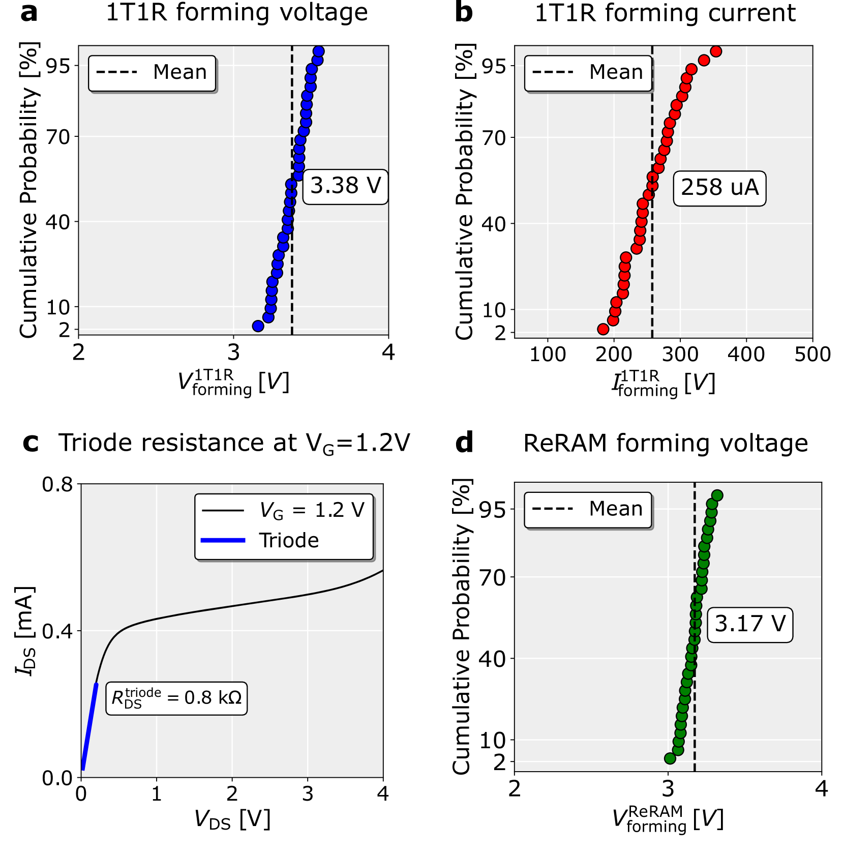
The image presents four separate plots characterizing the forming behavior of different resistive switching devices. Plots (a) and (d) show cumulative probability distributions of forming voltages for 1T1R and ReRAM devices, respectively. Plot (b) shows the cumulative probability distribution of forming current for 1T1R devices. Plot (c) displays an IV curve demonstrating the triode resistance of a device at a fixed gate voltage.
### Components/Axes
* **Plot a: 1T1R forming voltage**
* X-axis: V<sup>1T1R</sup><sub>forming</sub> [V] (Forming Voltage for 1T1R device) - Scale: 2 to 4 V
* Y-axis: Cumulative Probability [%] - Scale: 0 to 100%
* Data Series: Blue dots representing the cumulative distribution. Dashed black line representing the mean.
* **Plot b: 1T1R forming current**
* X-axis: I<sup>1T1R</sup><sub>forming</sub> [µA] (Forming Current for 1T1R device) - Scale: 100 to 500 µA
* Y-axis: Cumulative Probability [%] - Scale: 0 to 100%
* Data Series: Red dots representing the cumulative distribution. Dashed black line representing the mean.
* **Plot c: Triode resistance at V<sub>G</sub>=1.2V**
* X-axis: V<sub>DS</sub> [V] (Drain-Source Voltage) - Scale: 0 to 4 V
* Y-axis: I<sub>DS</sub> [mA] (Drain-Source Current) - Scale: 0 to 0.8 mA
* Data Series: Blue line representing the IV curve.
* **Plot d: ReRAM forming voltage**
* X-axis: V<sup>ReRAM</sup><sub>forming</sub> [V] (Forming Voltage for ReRAM device) - Scale: 2 to 4 V
* Y-axis: Cumulative Probability [%] - Scale: 0 to 100%
* Data Series: Green dots representing the cumulative distribution. Dashed black line representing the mean.
### Detailed Analysis or Content Details
* **Plot a: 1T1R forming voltage**
* The blue data points show a steep increase in cumulative probability between approximately 3.1 V and 3.5 V.
* The mean forming voltage is indicated by a dashed black line at approximately 3.38 V.
* **Plot b: 1T1R forming current**
* The red data points show a steep increase in cumulative probability between approximately 200 µA and 300 µA.
* The mean forming current is indicated by a dashed black line at approximately 258 µA.
* **Plot c: Triode resistance at V<sub>G</sub>=1.2V**
* The blue line shows a non-linear relationship between V<sub>DS</sub> and I<sub>DS</sub>.
* The current increases rapidly from 0 mA to approximately 0.4 mA as V<sub>DS</sub> increases from 0 V to 3 V.
* The triode resistance is labeled as approximately 0.8 kΩ.
* **Plot d: ReRAM forming voltage**
* The green data points show a steep increase in cumulative probability between approximately 3.0 V and 3.3 V.
* The mean forming voltage is indicated by a dashed black line at approximately 3.17 V.
### Key Observations
* The 1T1R devices exhibit forming voltages clustered around 3.38 V and forming currents clustered around 258 µA.
* The ReRAM devices exhibit forming voltages clustered around 3.17 V.
* The IV curve in plot (c) demonstrates a clear triode region with a resistance of 0.8 kΩ at V<sub>G</sub> = 1.2 V.
* All cumulative distribution plots show a relatively narrow distribution of forming voltages/currents, suggesting a consistent forming process.
### Interpretation
The data suggests that the 1T1R and ReRAM devices have different forming voltage requirements. The 1T1R devices require slightly higher forming voltages (mean of 3.38 V) compared to the ReRAM devices (mean of 3.17 V). The forming current distribution for 1T1R devices is also relatively narrow, indicating a consistent forming process. The IV curve in plot (c) provides insight into the device's behavior in the triode region, which is crucial for understanding its switching characteristics. The consistent forming characteristics, as indicated by the steep cumulative distributions, suggest a reliable and repeatable fabrication process. The difference in forming voltages between 1T1R and ReRAM could be attributed to differences in their material properties and device structures. The triode resistance value provides a key parameter for modeling and simulating the device's performance.