## Circuit Diagram and Transfer Characteristics
### Overview
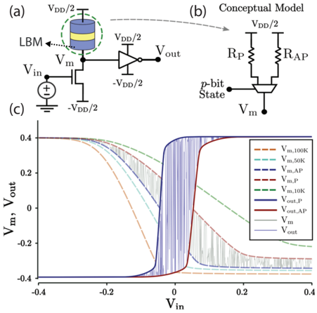
The image presents a circuit diagram involving a magnetic tunnel junction (MTJ) or LBM (likely Barrier Material), a conceptual model of the circuit, and a plot of the transfer characteristics (Vm, Vout vs. Vin) for different resistance states.
### Components/Axes
* **(a) Circuit Diagram:**
* LBM (Magnetic Tunnel Junction): Represented as a cylinder with two layers of different colors.
* Transistor: An NMOS transistor with the gate connected to Vm, source connected to -VDD/2, and drain connected to the LBM.
* Inverter: An inverter with input VDD/2 and -VDD/2, and output Vout.
* Voltage Source: Vin connected to ground.
* **(b) Conceptual Model:**
* Resistors: Two resistors, Rp and RAP, connected in series.
* p-bit State: A switch controlled by the p-bit state, connecting either Rp or RAP to Vm.
* Voltage Source: VDD/2
* **(c) Transfer Characteristics:**
* X-axis: Vin (Input Voltage), ranging from -0.4 to 0.4.
* Y-axis: Vm, Vout (Output Voltages), ranging from -0.4 to 0.4.
* Legend (Top-Right):
* Vm,100K (dashed orange)
* Vm,50K (dashed cyan)
* Vm,AP (dashed dark blue)
* Vm,P (dashed dark red)
* Vm,10K (dashed green)
* Vout,P (solid dark blue)
* Vout,AP (solid dark red)
* Vm (solid gray)
* Vout (solid light gray)
### Detailed Analysis or Content Details
* **Circuit Diagram (a):**
* The circuit consists of an LBM connected to an NMOS transistor and an inverter. The input voltage Vin controls the transistor, which in turn affects the voltage Vm at the LBM. The inverter outputs Vout based on Vm.
* **Conceptual Model (b):**
* The conceptual model simplifies the LBM as a switch between two resistors, Rp (parallel) and RAP (anti-parallel), representing different resistance states of the MTJ.
* **Transfer Characteristics (c):**
* **Vm,100K (dashed orange):** Starts at approximately 0.4 for Vin = -0.4, gradually decreases to approximately -0.4 as Vin increases to 0.4.
* **Vm,50K (dashed cyan):** Starts at approximately 0.4 for Vin = -0.4, gradually decreases to approximately -0.4 as Vin increases to 0.4.
* **Vm,AP (dashed dark blue):** Starts at approximately 0.4 for Vin = -0.4, gradually decreases to approximately -0.4 as Vin increases to 0.4.
* **Vm,P (dashed dark red):** Starts at approximately 0.4 for Vin = -0.4, gradually decreases to approximately -0.4 as Vin increases to 0.4.
* **Vm,10K (dashed green):** Starts at approximately 0.4 for Vin = -0.4, gradually decreases to approximately -0.4 as Vin increases to 0.4.
* **Vout,P (solid dark blue):** Remains at approximately 0.4 until Vin reaches approximately -0.05, then rapidly decreases to approximately -0.4 as Vin increases to 0.05, and remains at -0.4 for higher Vin values.
* **Vout,AP (solid dark red):** Remains at approximately -0.4 until Vin reaches approximately -0.05, then rapidly increases to approximately 0.4 as Vin increases to 0.05, and remains at 0.4 for higher Vin values.
* **Vm (solid gray):** Similar to Vout,P, but with less sharp transitions.
* **Vout (solid light gray):** Similar to Vout,AP, but with less sharp transitions.
### Key Observations
* The Vm curves for different resistance values (100K, 50K, AP, P, 10K) show a gradual transition from high to low voltage as Vin increases.
* The Vout curves (Vout,P and Vout,AP) exhibit a sharp transition, indicating a switching behavior.
* The Vout,P and Vout,AP curves are inverted with respect to each other, suggesting complementary outputs based on the resistance state of the LBM.
### Interpretation
The image illustrates the operation of a memory cell based on a magnetic tunnel junction (MTJ). The circuit diagram shows how the MTJ is integrated with a transistor and an inverter to create a memory element. The conceptual model simplifies the MTJ as a switch between two resistance states, which are then used to generate different output voltages. The transfer characteristics demonstrate the switching behavior of the circuit, where the output voltage changes sharply based on the input voltage and the resistance state of the MTJ. The different Vm curves for different resistance values likely represent different intermediate states or variations in the MTJ's resistance. The sharp transitions in Vout,P and Vout,AP indicate that the circuit can be used to reliably store and read binary data.