## Circuit Diagram and Voltage Transfer Characteristics
### Overview
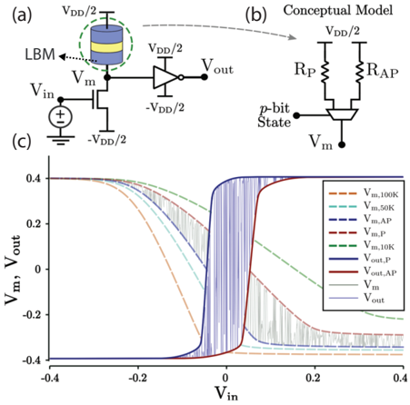
The image presents a technical schematic of a p-bit circuit (a) and its conceptual model (b), accompanied by voltage transfer characteristics (c). The diagram illustrates a loop-based memory (LBM) circuit with voltage inputs/outputs, while the graph shows the relationship between input voltage (V_in) and memory/output voltages (V_m, V_out) under varying conditions.
### Components/Axes
**Diagram (a):**
- **LBM Circuit**: Contains a loop with a yellow band (likely a resistive element), connected to:
- **V_in**: Input voltage source
- **V_m**: Memory voltage node
- **V_out**: Output voltage node
- **V_dd/2**: Half of the supply voltage (reference point)
- **Conceptual Model (b)**:
- **p-bit State**: Simplified representation with:
- **R_P**: Parallel resistance
- **R_AP**: Anti-parallel resistance
- **V_m**: Memory voltage source
- **V_dd/2**: Supply voltage reference
**Graph (c):**
- **X-axis**: Input voltage (V_in) ranging from -0.4 to +0.4
- **Y-axis**: Memory voltage (V_m) and Output voltage (V_out), both ranging from -0.4 to +0.4
- **Legend**:
- Solid lines: V_m values (e.g., V_m100K, V_m50K, V_m10K, V_m1P)
- Dashed lines: V_out values (e.g., V_out_P, V_out_AP)
- Dotted lines: Reference voltages (V_m, V_out)
### Detailed Analysis
**Graph Trends**:
1. **V_m (Solid Lines)**:
- Sharp transition at V_in ≈ 0 (hysteresis-like behavior)
- Higher V_m values (e.g., V_m100K) show wider hysteresis loops
- Lower V_m values (e.g., V_m1P) exhibit narrower transitions
2. **V_out (Dashed Lines)**:
- Step-like transitions at V_in ≈ ±0.2
- V_out_P (blue dashed) and V_out_AP (red dashed) show complementary switching
3. **Reference Lines (Dotted)**:
- V_m (gray) and V_out (black) form baseline thresholds
**Key Observations**:
- **Hysteresis Effect**: V_m shows memory retention (non-linear response to V_in)
- **Bistable Behavior**: V_out_P and V_out_AP represent distinct states (parallel/anti-parallel)
- **Voltage Scaling**: Higher V_m values correlate with broader hysteresis ranges
- **Symmetry**: V_in = 0 acts as a critical threshold for state switching
### Interpretation
The circuit demonstrates a **p-bit** (programmable bit) functionality, where:
1. **LBM Circuit (a)**:
- The yellow band in the loop likely represents a resistive memory element (e.g., RRAM)
- V_m controls the memory state via voltage-dependent resistance
- V_out reflects the output state (parallel/anti-parallel configuration)
2. **Conceptual Model (b)**:
- R_P and R_AP represent the two stable resistance states of the memory element
- V_m acts as a control voltage to switch between states
- V_dd/2 provides a reference for bipolar switching
3. **Graph (c)**:
- The sharp transitions confirm **threshold-based switching** (typical of memristive devices)
- Hysteresis in V_m suggests **non-volatility** (retains state without power)
- Complementary V_out_P/V_out_AP indicates **bistable logic** (0/1 states)
**Technical Implications**:
- The system implements **analog-to-digital conversion** via voltage thresholds
- Hysteresis enables **error-resistant memory** (resists noise-induced state changes)
- The p-bit architecture supports **in-memory computing** (data processing within memory cells)
**Uncertainties**:
- Exact resistance values (R_P, R_AP) are not quantified
- Temperature dependence of V_m is implied but not explicitly modeled
- Non-ideal effects (e.g., leakage currents) are not shown in the schematic