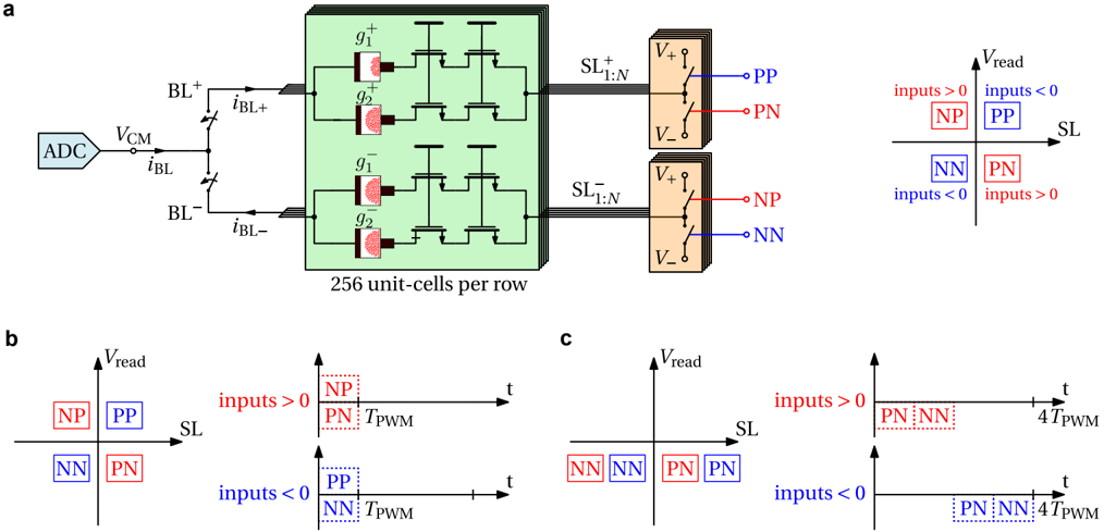
## Circuit Diagram and Signal Representation
### Overview
The image presents a circuit diagram coupled with signal representations illustrating the behavior of a memory cell array. The diagram is divided into three parts (a, b, and c). Part (a) shows the circuit architecture, including the memory cell array, bit lines, sense lines, and ADC. Parts (b) and (c) depict signal representations (Vread vs. SL and Vread vs. time) under different input conditions (inputs > 0 and inputs < 0).
### Components/Axes
**Part (a): Circuit Diagram**
* **ADC:** Analog-to-Digital Converter.
* **VCM:** Common-mode voltage.
* **BL+:** Bit line positive.
* **BL-:** Bit line negative.
* **iBL+:** Current in the positive bit line.
* **iBL-:** Current in the negative bit line.
* **g1+, g2, g1-, g2:** Conductance elements within the memory cell array.
* **Memory Cell Array:** A green block containing transistors and conductance elements, labeled "256 unit-cells per row."
* **SL1:N+:** Sense line positive.
* **SL1:N-:** Sense line negative.
* **V+:** Positive voltage.
* **V-:** Negative voltage.
* **PP:** Positive-Positive output. (Blue)
* **PN:** Positive-Negative output. (Red)
* **NP:** Negative-Positive output. (Red)
* **NN:** Negative-Negative output. (Blue)
**Part (b): Signal Representation 1**
* **Axes:** Vread (vertical axis) vs. SL (horizontal axis), and Vread (vertical axis) vs. t (time axis).
* **Input Conditions:** "inputs > 0" (red) and "inputs < 0" (blue).
* **Time Period:** TPWM.
* **Quadrants (Vread vs. SL):**
* Top-left: NP (Red)
* Top-right: PP (Blue)
* Bottom-left: NN (Blue)
* Bottom-right: PN (Red)
**Part (c): Signal Representation 2**
* **Axes:** Vread (vertical axis) vs. SL (horizontal axis), and Vread (vertical axis) vs. t (time axis).
* **Input Conditions:** "inputs > 0" (red) and "inputs < 0" (blue).
* **Time Period:** 4TPWM.
* **Quadrants (Vread vs. SL):**
* Top-left: NN (Red)
* Top-right: PN (Blue)
* Bottom-left: NN (Blue)
* Bottom-right: PN (Red)
### Detailed Analysis or ### Content Details
**Part (a): Circuit Diagram**
* The ADC measures the difference between the currents iBL+ and iBL-.
* The memory cell array consists of 256 unit cells per row.
* The sense lines SL+ and SL- are connected to switches controlled by voltages V+ and V-.
* The outputs PP, PN, NP, and NN are generated based on the switching configuration.
**Part (b): Signal Representation 1**
* **Vread vs. SL:**
* When inputs > 0, the output is PN (bottom-right quadrant).
* When inputs < 0, the output is NN (bottom-left quadrant).
* **Vread vs. t:**
* When inputs > 0, Vread alternates between NP and PN over the time period TPWM.
* When inputs < 0, Vread alternates between PP and NN over the time period TPWM.
**Part (c): Signal Representation 2**
* **Vread vs. SL:**
* When inputs > 0, the output is PN (bottom-right quadrant).
* When inputs < 0, the output is NN (bottom-left quadrant).
* **Vread vs. t:**
* When inputs > 0, Vread alternates between PN and NN over the time period 4TPWM.
* When inputs < 0, Vread alternates between PN and NN over the time period 4TPWM.
### Key Observations
* The circuit diagram shows the architecture of a memory cell array with sensing circuitry.
* The signal representations illustrate how the output voltage (Vread) varies with the sense line (SL) and time (t) based on the input conditions.
* The quadrants in the Vread vs. SL plots indicate the expected output polarity for different input conditions.
* The Vread vs. t plots show the temporal behavior of the output voltage, alternating between different polarity states.
### Interpretation
The image provides a comprehensive view of a memory cell array's operation. The circuit diagram shows the physical connections and components, while the signal representations illustrate the expected behavior of the output voltage under different input conditions. The alternating polarity states in the Vread vs. t plots suggest a dynamic or switching behavior of the memory cell. The relationship between the input polarity and the output polarity is clearly demonstrated in the Vread vs. SL plots. The use of TPWM and 4TPWM suggests different operating modes or timing schemes for the memory cell.