\n
## Diagram: Memory Cell Operation with Timing Diagrams
### Overview
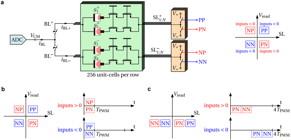
The image presents a schematic diagram of a memory cell array and associated circuitry, along with timing diagrams illustrating its operation. The diagram details the read operation of a memory cell, showing how input signals affect the read voltage and timing. It appears to be related to a non-volatile memory technology. The diagram is divided into three parts: (a) a schematic of the memory cell array and read circuitry, (b) a timing diagram for positive inputs, and (c) a timing diagram for negative inputs.
### Components/Axes
**Part (a):**
* **Labels:** BL+, BL-, Vcm, iBL+, iBL-, ADC, g1+, g1-, g2+, g2-, SL1:N, SLT:N, V+, V-, PP, PN, NP, NN, 256 unit-cells per row.
* **Components:** ADC (Analog-to-Digital Converter), Bitlines (BL+, BL-), Memory Cell Array (represented by the green blocks), Select Lines (SL1:N, SLT:N), Voltage Sources (V+, V-), Output Nodes (PP, PN, NP, NN).
* **Diagrammatic Elements:** Transistors within the memory cells, connections between cells and bitlines, connections to select lines and voltage sources.
**Parts (b) & (c):**
* **Axes:** Vertical axis represents Vread (Read Voltage), Horizontal axis represents time (t).
* **Labels:** SL (Select Line), inputs > 0, inputs < 0, TPWM (Pulse Width Modulation period), 4TPWM.
* **States:** NP, PP, PN, NN.
### Detailed Analysis or Content Details
**Part (a):**
The diagram shows a memory cell array consisting of 256 unit cells per row. Each unit cell contains two transistors (g1+, g1- and g2+, g2-). The bitlines BL+ and BL- are connected to the cells. The select lines SL1:N and SLT:N control access to the cells. The output nodes PP, PN, NP, and NN are connected to the cells through the transistors and select lines. The ADC converts the analog signal from the bitlines to a digital value.
**Part (b):**
This timing diagram illustrates the read operation when inputs are greater than 0.
* When inputs > 0, the Vread signal rises during the SL activation.
* The PP state is activated during the SL activation, with a pulse width of TPWM.
* When inputs < 0, the Vread signal remains low.
* The NN state is activated during the SL activation, with a pulse width of TPWM.
**Part (c):**
This timing diagram illustrates the read operation when inputs are less than 0.
* When inputs > 0, the Vread signal rises during the SL activation.
* The PN state is activated during the SL activation, with a pulse width of 4TPWM.
* When inputs < 0, the Vread signal remains low.
* The NN state is activated during the SL activation, with a pulse width of 4TPWM.
### Key Observations
* The timing diagrams (b) and (c) show that the read voltage (Vread) is affected by the input signal.
* The activation of the states (PP, PN, NP, NN) is synchronized with the select line (SL) activation.
* The pulse width of the activation signal (TPWM) varies depending on the input signal. Specifically, the pulse width is 4TPWM when inputs are > 0 in part (c) and TPWM when inputs are > 0 in part (b).
* The diagram suggests a differential sensing scheme, as both positive and negative inputs are considered.
### Interpretation
The diagram illustrates the operation of a memory cell array with a read mechanism that utilizes pulse width modulation (PWM) to encode information. The different states (PP, PN, NP, NN) likely represent different charge levels or states within the memory cells. The timing diagrams demonstrate how the read voltage changes based on the input signal and the activation of the select line. The variation in pulse width (TPWM vs. 4TPWM) suggests a method for distinguishing between different input values. The ADC converts the analog signal from the bitlines into a digital representation of the stored data. The diagram suggests a non-volatile memory technology where the state of the memory cell is retained even when power is removed. The use of select lines and differential sensing indicates a robust and efficient read operation. The diagram is a high-level representation of the memory cell operation and does not provide specific details about the materials or fabrication process. The diagram is a conceptual illustration of the memory cell operation and does not provide specific numerical data.