TECHNICAL ASSET FINGERPRINT
85065075de5dc7a8fb628d7b
Click to view fullscreen
Press ESC or click to close
FOUND IN PAPERS
EXPERT: healer-alpha-free VERSION 1
RUNTIME: free/openrouter/healer-alpha
INTEL_VERIFIED
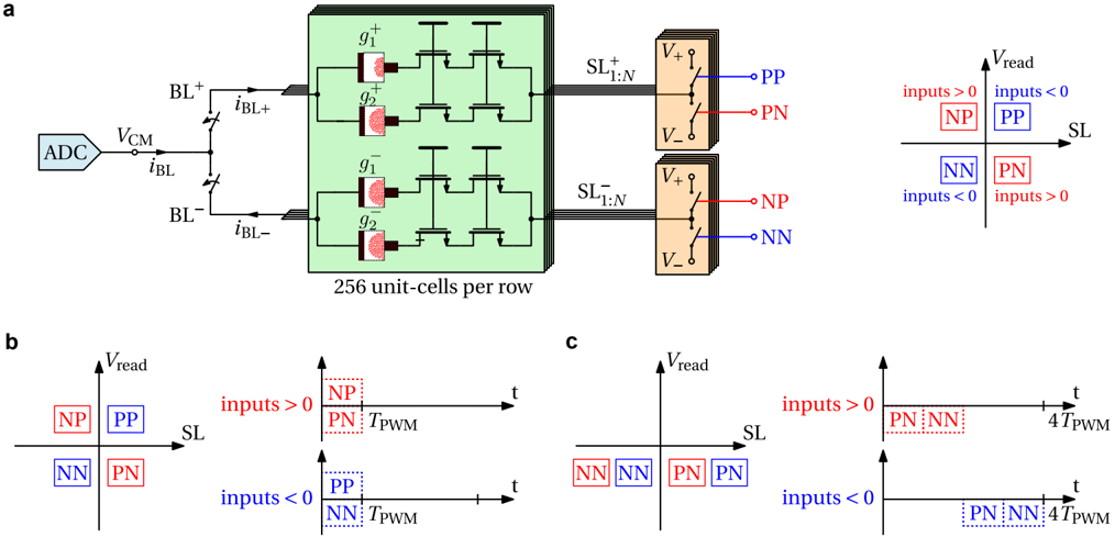
## Circuit Diagram: Differential Sensing and PWM Modulation Scheme for a Memory/Compute Array
### Overview
The image is a multi-part technical diagram (labeled a, b, c) illustrating a differential sensing scheme and pulse-width modulation (PWM) timing for a resistive memory or compute-in-memory array. It details how input signals (positive/negative) are mapped to specific output states (NP, PP, NN, PN) and how these states are read over time.
### Components/Axes
**Part a: System Architecture**
* **Left Block (ADC & Bitlines):**
* An Analog-to-Digital Converter (`ADC`) is connected to a common-mode voltage (`V_CM`).
* Two differential bitlines: `BL+` and `BL-`.
* Currents are labeled `i_BL+`, `i_BL`, and `i_BL-`.
* **Central Block (Memory/Compute Array):**
* A green block containing a 2x2 grid of unit cells.
* Each unit cell contains a resistive element (red circle with a gradient) and two transistors.
* The resistive elements are labeled `g₁⁺`, `g₂⁺`, `g₁⁻`, `g₂⁻`.
* A label below states: "256 unit-cells per row".
* The array is connected to two sets of source lines: `SL₁:N⁺` (top) and `SL₁:N⁻` (bottom).
* **Right Block (Switching/Output Logic):**
* Two blocks connected to the source lines.
* Each block has switches connecting to positive (`V+`) and negative (`V-`) supply voltages.
* The top block outputs to terminals labeled `PP` (blue) and `PN` (red).
* The bottom block outputs to terminals labeled `NP` (red) and `NN` (blue).
* **Legend (Top-Right of Part a):**
* A 2x2 quadrant plot with axes: Vertical = `V_read`, Horizontal = `SL`.
* Quadrants are labeled with state codes and input conditions:
* Top-Left (Red): `NP` (inputs > 0)
* Top-Right (Blue): `PP` (inputs < 0)
* Bottom-Left (Blue): `NN` (inputs < 0)
* Bottom-Right (Red): `PN` (inputs > 0)
**Part b: Timing Diagram for Standard PWM**
* **Left Plot:** A repeat of the `V_read` vs. `SL` quadrant legend from part a.
* **Right Plot (Timing):**
* Horizontal axis: Time (`t`).
* Vertical axis: Implicitly represents signal state (high/low).
* Two scenarios are shown:
1. **Top (inputs > 0):** A red dashed box labeled `NP` is high for a duration `T_PWM`. A red dashed box labeled `PN` is low.
2. **Bottom (inputs < 0):** A blue dashed box labeled `PP` is high for a duration `T_PWM`. A blue dashed box labeled `NN` is low.
**Part c: Timing Diagram for Extended PWM**
* **Left Plot:** A modified quadrant legend. The horizontal axis is `SL`. The vertical axis is `V_read`. The quadrants now show:
* Left side: `NN` (blue) and `NN` (blue).
* Right side: `PN` (red) and `PN` (red).
* **Right Plot (Timing):**
* Horizontal axis: Time (`t`).
* Two scenarios are shown:
1. **Top (inputs > 0):** A red dashed box labeled `PN` is high, followed by a red dashed box labeled `NN` being high. The total period is `4 T_PWM`.
2. **Bottom (inputs < 0):** A blue dashed box labeled `PN` is low, followed by a blue dashed box labeled `NN` being low. The total period is `4 T_PWM`.
### Detailed Analysis
**Part a - Signal Flow and State Mapping:**
1. The system reads from a row of 256 unit cells via differential bitlines (`BL+`, `BL-`) into an ADC.
2. The state of the unit cells (`g` values) and the applied source line (`SL`) voltages determine the output.
3. The legend defines a mapping from input polarity and the `SL`/`V_read` operating point to one of four output states:
* **NP (Negative-Positive):** Activated when inputs > 0 and the operating point is in the top-left quadrant (high `V_read`, low `SL`).
* **PP (Positive-Positive):** Activated when inputs < 0 and the operating point is in the top-right quadrant (high `V_read`, high `SL`).
* **NN (Negative-Negative):** Activated when inputs < 0 and the operating point is in the bottom-left quadrant (low `V_read`, low `SL`).
* **PN (Positive-Negative):** Activated when inputs > 0 and the operating point is in the bottom-right quadrant (low `V_read`, high `SL`).
**Part b - Standard PWM Timing:**
* For a given input polarity, only one of the two possible states (from the legend) is activated for a pulse width of `T_PWM`.
* **inputs > 0:** The `NP` state is pulsed high.
* **inputs < 0:** The `PP` state is pulsed high.
* The complementary state (`PN` for inputs>0, `NN` for inputs<0) remains low during this pulse.
**Part c - Extended PWM Timing:**
* This shows a different modulation scheme over a longer period (`4 T_PWM`).
* The quadrant mapping is simplified: the left side of the `SL` axis corresponds to `NN` states, and the right side corresponds to `PN` states.
* **inputs > 0:** The sequence is `PN` (high) followed by `NN` (high).
* **inputs < 0:** The sequence is `PN` (low) followed by `NN` (low). This suggests the signal polarity is inverted compared to the `inputs > 0` case.
### Key Observations
1. **Differential Architecture:** The entire design is fully differential, from bitlines (`BL+`/`BL-`) to source lines (`SL⁺`/`SL⁻`) and output states (e.g., `PP` vs. `NN`).
2. **State Encoding:** Information is encoded in a combination of analog levels (`V_read`, `SL`) and digital pulses (`T_PWM`). The four states (`NP`, `PP`, `NN`, `PN`) likely represent the four possible combinations of two binary inputs.
3. **Input Polarity Dictates State Selection:** The primary factor determining which pair of states is active is the sign of the input (`inputs > 0` or `inputs < 0`). The specific quadrant (determined by `V_read` and `SL`) then selects the exact state within that pair.
4. **Timing Variation:** Part b uses a single pulse (`T_PWM`), while part c uses a sequence over `4 T_PWM`, indicating different operational modes or encoding schemes (e.g., for different precision or noise immunity).
5. **Visual Consistency:** Color coding is used consistently: Red for states associated with `inputs > 0` (`NP`, `PN`) and Blue for states associated with `inputs < 0` (`PP`, `NN`).
### Interpretation
This diagram describes the readout and modulation scheme for a differential, non-volatile memory array (like RRAM or MRAM) configured for analog computing or neuromorphic applications.
* **Function:** The system appears to perform a multiply-accumulate (MAC) operation. The conductance states (`g`) of the unit cells represent weights. Applying input voltages (implied on the `SL` lines) generates currents that are summed on the bitlines and digitized by the ADC.
* **Role of the Four States:** The `NP`, `PP`, `NN`, `PN` states likely represent the sign and magnitude of the computed result. For example, they could correspond to the four quadrants of a signed output, where the first letter is the sign of the first input and the second letter is the sign of the second input in a differential pair.
* **PWM as an Encoding Method:** Using pulse-width modulation (`T_PWM`) is a common technique in analog computing to represent analog values in the time domain, offering better noise immunity and linearity than pure voltage or current levels. The extended timing in part c might be for a higher-resolution or multi-bit conversion step.
* **System Integration:** The diagram connects the core memory array (center) to peripheral circuits: the ADC for sensing (left) and the switching logic for applying read voltages and routing outputs (right). This represents a complete subsystem for in-memory computation.
**Language:** All text in the image is in English.
DECODING INTELLIGENCE...