## Block Diagram and Timing Diagrams: Memory Array and Read/Write Operations
### Overview
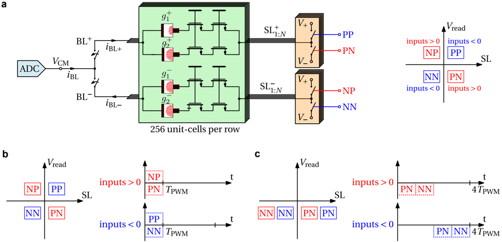
The image consists of three technical diagrams:
1. **Part a**: A block diagram of a memory array with 256 unit-cells per row, showing signal routing and control logic.
2. **Part b**: A timing diagram illustrating read/write operations with voltage thresholds (V_read) and input conditions.
3. **Part c**: A modified timing diagram with additional pulse-width modulation (PWM) annotations.
---
### Components/Axes
#### Part a (Block Diagram)
- **Key Components**:
- **ADC**: Analog-to-Digital Converter (left side).
- **BL+ / BL-**: Bitline inputs (connected to ADC).
- **VCM**: Voltage-controlled memory (central green block).
- **256 unit-cells per row**: Array of memory cells (green block).
- **SL+ / SL-**: Select lines (right side, connected to V+ and V-).
- **NP / PP / NN / PN**: Memory states (labeled in a matrix on the right).
- **Axes/Legends**:
- **V_read**: Read voltage axis (vertical, right side).
- **Legend**:
- **NP**: Red (Negative-Positive).
- **PP**: Blue (Positive-Positive).
- **NN**: Green (Negative-Negative).
- **PN**: Orange (Positive-Negative).
- **SL**: Gray (Select Line).
#### Part b (Timing Diagram)
- **Axes**:
- **V_read**: Vertical axis (voltage).
- **t**: Time axis (horizontal).
- **Legend**:
- **NP**: Red.
- **PP**: Blue.
- **SL**: Gray.
- **NN**: Green.
- **PN**: Orange.
- **Lines**:
- **Inputs > 0**: Red (NP) and Blue (PP) lines.
- **Inputs < 0**: Green (NN) and Orange (PN) lines.
- **T_PWM**: Pulse-width modulation period (annotated on lines).
#### Part c (Timing Diagram)
- **Axes**: Same as Part b.
- **Legend**: Same as Part b.
- **Lines**:
- **Inputs > 0**: Orange (PN) and Green (NN) lines.
- **Inputs < 0**: Blue (PP) and Red (NP) lines.
- **4T_PWM**: Extended pulse-width modulation period (annotated on lines).
---
### Detailed Analysis
#### Part a
- **Signal Flow**:
- ADC outputs **i_BL+** and **i_BL-** control the green memory array.
- The array connects to **SL+** and **SL-** via **V+** and **V-** rails.
- The right-side matrix maps memory states (NP, PP, NN, PN) to **V_read** thresholds.
- **Spatial Grounding**:
- **Legend** is positioned to the right of the matrix.
- **SL+** and **SL-** are stacked vertically on the right.
#### Part b
- **Trends**:
- **Inputs > 0**:
- **NP** (red) slopes upward.
- **PP** (blue) slopes downward.
- **Inputs < 0**:
- **NN** (green) slopes upward.
- **PN** (orange) slopes downward.
- **T_PWM**: Periodicity indicated by dashed lines.
#### Part c
- **Trends**:
- **Inputs > 0**:
- **PN** (orange) slopes upward.
- **NN** (green) slopes downward.
- **Inputs < 0**:
- **PP** (blue) slopes upward.
- **NP** (red) slopes downward.
- **4T_PWM**: Longer periodicity (4× T_PWM) indicated by dashed lines.
---
### Key Observations
1. **Part a**: The memory array uses differential signaling (BL+/BL-) and select lines (SL+/SL-) to address unit-cells.
2. **Part b/c**: Timing diagrams show voltage thresholds (V_read) changing over time based on input polarity.
3. **PWM Annotations**: T_PWM and 4T_PWM suggest modulation of read/write pulses for stability or error correction.
---
### Interpretation
- **Part a** represents a **non-volatile memory array** (e.g., PCM or MRAM) with 256 cells per row. The block diagram emphasizes differential signaling for noise immunity.
- **Parts b/c** illustrate **read/write timing protocols**:
- **Input polarity** determines memory state transitions (e.g., NP/PP for positive inputs, NN/PN for negative inputs).
- **PWM modulation** (T_PWM, 4T_PWM) likely controls write/erase cycles to prevent overvoltage damage.
- **Critical Insight**: The system uses **voltage thresholds** (V_read) to distinguish memory states, with timing diagrams optimizing pulse duration for reliability.
---
*Note: No numerical data points are explicitly labeled; trends are inferred from line slopes and annotations.*