TECHNICAL ASSET FINGERPRINT
8fb58081a5a6b56f2c3a526f
Click to view fullscreen
Press ESC or click to close
FOUND IN PAPERS
EXPERT: healer-alpha-free VERSION 1
RUNTIME: free/openrouter/healer-alpha
INTEL_VERIFIED
## Technical Diagram and Chart Analysis
### Overview
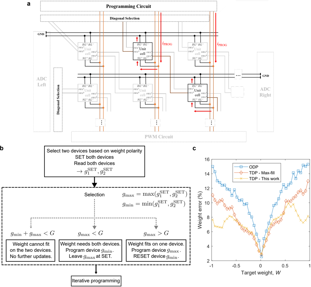
The image is a composite technical figure containing three distinct parts labeled **a**, **b**, and **c**. It appears to describe a hardware system for programming and verifying weights in a resistive memory or neuromorphic computing array, along with a performance evaluation chart.
### Components/Axes
**Part a: Circuit Diagram**
* **Title/Label:** "Programming Circuit" (top center).
* **Major Blocks:**
* "Programming Circuit" (top, dashed box).
* "Diagonal Selection" (two instances, dashed boxes).
* "ADC Left" and "ADC Right" (left and right sides, dashed boxes).
* "PWM Circuit" (bottom, dashed box).
* **Unit Cell Structure:** Multiple identical "Unit cell" blocks are shown. Each contains internal labels:
* `BL+`, `BL-` (Bit Lines)
* `SEL+`, `SEL-` (Select Lines)
* `SL+`, `SL-` (Source Lines)
* **Signals & Connections:**
* `GND` (Ground) lines are shown at the top and right.
* `i_PROG` (Programming Current) is indicated with red arrows pointing downward into two unit cells.
* Orange lines represent connections from the "PWM Circuit" to the unit cells.
* Black lines represent other control and data paths.
* Ellipses (`...`) indicate the array extends further.
**Part b: Flowchart**
* **Process Flow:** A top-down flowchart describing an algorithm.
* **Text Blocks (in order):**
1. "Select two devices based on weight polarity"
2. "SET both devices"
3. "Read both devices"
4. "→ g₁^SET, g₂^SET"
5. "Selection" (central node)
6. "g_max = max(g₁^SET, g₂^SET)"
7. "g_min = min(g₁^SET, g₂^SET)"
* **Decision Logic (Three branches from "Selection"):**
* **Condition 1:** "g_min + g_max < G"
* **Outcome:** "Weight cannot fit on the two devices. No further updates."
* **Condition 2:** "g_max < G"
* **Outcome:** "Weight needs both devices. Program device g_min. Leave g_max at SET."
* **Condition 3:** "g_max > G"
* **Outcome:** "Weight fits on one device. Program device g_max. RESET device g_min."
* **Final Step:** All branches lead to "Iterative programming".
**Part c: Line Chart**
* **Chart Type:** Line chart with markers.
* **X-Axis:**
* **Label:** "Target weight, W"
* **Scale:** Linear, from -1 to 1. Major ticks at -1, -0.5, 0, 0.5, 1.
* **Y-Axis:**
* **Label:** "Weight error (%)"
* **Scale:** Linear, from 2 to 16. Major ticks at 2, 4, 6, 8, 10, 12, 14, 16.
* **Legend (Top-Left Corner):**
* **Blue line with square markers:** "ODP"
* **Orange line with diamond markers:** "TDP - Max-fill"
* **Yellow line with 'x' markers:** "TDP - This work"
### Detailed Analysis
**Part a: Circuit Operation**
The diagram illustrates a programming scheme for a crossbar-like array of memory cells. The "Programming Circuit" and "PWM Circuit" provide the necessary signals. "Diagonal Selection" logic appears to activate specific unit cells. The red `i_PROG` arrows indicate that programming current is injected into selected cells. The presence of "ADC Left" and "ADC Right" suggests readout circuitry for measuring cell states (conductance).
**Part b: Algorithm Logic**
The flowchart details a "TDP" (likely Two-Device Programming) algorithm. It uses a pair of devices (with conductances g₁^SET and g₂^SET) to represent a single target weight. The core logic compares the sum and maximum of the two conductances against a threshold `G` to decide how to program the weight: using both devices, using one device (and resetting the other), or deeming the weight unrepresentable.
**Part c: Performance Data**
* **Trend Verification:**
* **ODP (Blue Squares):** Forms a symmetric "V" shape. Error is highest (~15%) at the extremes (W = -1 and W = 1) and lowest (~2.5%) at the center (W = 0).
* **TDP - Max-fill (Orange Diamonds):** Also forms a "V" shape but is consistently lower than ODP. Error ranges from ~11% at W = -1 to a minimum of ~2.5% at W = 0, then back to ~13% at W = 1.
* **TDP - This work (Yellow 'x's):** Shows a different, flatter profile. Error is relatively stable between ~6% and 8% across the entire range of W, with a slight dip near W = 0 (~3%). It has the lowest error for |W| > 0.2 approximately.
* **Key Data Points (Approximate):**
* At W = -1: ODP ~15%, TDP-Max-fill ~11%, TDP-This work ~7.5%.
* At W = 0: All methods converge to a minimum error of ~2.5-3%.
* At W = 1: ODP ~15%, TDP-Max-fill ~13%, TDP-This work ~8%.
### Key Observations
1. **Spatial Layout:** The legend in chart **c** is placed in the top-left quadrant, avoiding overlap with the data lines which are concentrated in the center and right.
2. **Symmetry:** The ODP and TDP-Max-fill error curves are roughly symmetric around W = 0, suggesting the programming error is a function of the weight's magnitude, not its sign.
3. **Performance Inversion:** The proposed method ("TDP - This work") trades off a slightly higher minimum error at W=0 for significantly improved (lower) error across most of the weight range, especially for larger magnitude weights. It eliminates the high-error "V" shape.
4. **Algorithm-Chart Link:** The flowchart in **b** explains the mechanism behind the "TDP" lines in chart **c**. The "ODP" likely stands for "One-Device Programming," serving as a baseline.
### Interpretation
This figure presents a complete technical narrative: a hardware architecture (**a**), a novel programming algorithm for that hardware (**b**), and empirical results proving the algorithm's superiority (**c**).
The data demonstrates that the proposed Two-Device Programming (TDP) method, particularly the variant labeled "This work," provides a more uniform and generally lower weight programming error compared to both One-Device Programming (ODP) and an alternative TDP strategy ("Max-fill"). The key innovation appears to be the decision logic in the flowchart that intelligently assigns weights to one or two devices based on conductance thresholds, avoiding the high-error regimes seen in the other methods at extreme weight values. This suggests the method is more robust and reliable for implementing neural networks or other analog computing tasks where accurate weight representation across a full range is critical. The circuit diagram confirms this is implemented in a scalable array architecture with peripheral programming and readout circuits.
DECODING INTELLIGENCE...