## Chip Layout: Neuromorphic Processor
### Overview
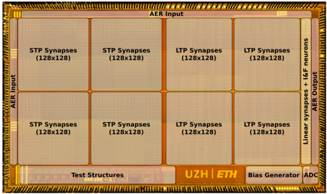
The image shows a layout of a neuromorphic processor chip. It consists of several functional blocks, including AER (Address Event Representation) input and output, STP (Short-Term Plasticity) and LTP (Long-Term Plasticity) synapses, linear synapses with integrate-and-fire (I&F) neurons, test structures, bias generator, and an ADC (Analog-to-Digital Converter). The chip is surrounded by a dense array of connection pads.
### Components/Axes
* **AER Input:** Located at the top and left side of the chip.
* **STP Synapses (128x128):** Four blocks of short-term plasticity synapses, each with a dimension of 128x128, are located in the top-left and bottom-left quadrants.
* **LTP Synapses (128x128):** Four blocks of long-term plasticity synapses, each with a dimension of 128x128, are located in the top-right and bottom-right quadrants.
* **Linear synapses + I&F neurons:** Located on the right side of the chip.
* **AER Output:** Located on the right side of the chip, next to the linear synapses and I&F neurons.
* **Test Structures:** Located at the bottom-left of the chip.
* **UZH ETH:** Located at the bottom-center of the chip. These are likely the logos of the University of Zurich (UZH) and ETH Zurich.
* **Bias Generator:** Located at the bottom-right of the chip.
* **ADC:** Located at the bottom-right of the chip, next to the Bias Generator.
### Detailed Analysis
The chip is divided into functional blocks. The AER input is present on the top and left edges, suggesting data input from multiple directions. The STP and LTP synapse blocks are arranged in a 2x2 grid in the top-left/bottom-left and top-right/bottom-right quadrants, respectively. Each synapse block has dimensions of 128x128. The linear synapses and I&F neurons are located on the right edge, followed by the AER output. The test structures, UZH/ETH logos, bias generator, and ADC are located at the bottom edge.
### Key Observations
* The chip is designed for neuromorphic computing, implementing both short-term and long-term plasticity.
* The AER interface suggests event-based communication.
* The presence of linear synapses and I&F neurons indicates a spiking neural network architecture.
* The inclusion of test structures and an ADC suggests a focus on characterization and analog signal processing.
### Interpretation
The chip layout indicates a neuromorphic processor designed for implementing spiking neural networks with both short-term and long-term plasticity. The AER interface allows for event-based communication, which is common in neuromorphic systems. The arrangement of the synapse blocks and neuron blocks suggests a modular architecture. The inclusion of test structures and an ADC indicates a focus on characterization and analog signal processing, which are important for developing and optimizing neuromorphic hardware. The presence of UZH and ETH logos suggests that the chip was developed in collaboration between the University of Zurich and ETH Zurich.