\n
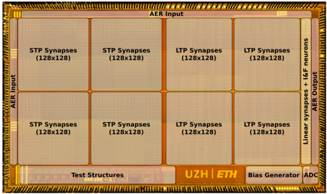
## Diagram: Neuromorphic Chip Layout
### Overview
The image depicts a layout of a neuromorphic chip, likely a microchip designed to mimic the structure and function of the human brain. The chip is divided into several rectangular blocks, each labeled with a specific function related to synaptic processing and neural networks. The overall structure appears to be highly regular and modular.
### Components/Axes
The diagram is organized into a grid-like structure with the following key components:
* **AER Input:** Located on the left side, vertically oriented.
* **AER Output:** Located on the right side, vertically oriented.
* **STP Synapses (128x128):** Four blocks labeled as such, arranged in a 2x2 grid in the top-left and bottom-left quadrants.
* **LTP Synapses (128x128):** Four blocks labeled as such, arranged in a 2x2 grid in the top-right and bottom-right quadrants.
* **Linear synapses + I&F neurons:** A vertical block on the far right.
* **Test Structures:** A horizontal block at the bottom-center.
* **Bias Generator:** A block at the bottom-right.
* **ADC:** A block at the bottom-right, adjacent to the Bias Generator.
* **UZH | ETH:** A logo/label at the bottom-center, between the Test Structures and the Bias Generator.
The dimensions (128x128) are consistently associated with the STP and LTP synapse blocks, likely representing the size of the synaptic array in terms of neurons or processing elements.
### Detailed Analysis / Content Details
The chip is divided into eight primary functional blocks, arranged in a 2x4 grid. The top row consists of two STP Synapse blocks and two LTP Synapse blocks. The bottom row mirrors this arrangement. The left and right edges are occupied by AER Input and AER Output blocks, respectively. The bottom edge contains Test Structures, a Bias Generator, and an ADC.
* **STP Synapses:** Four blocks, each labeled "STP Synapses (128x128)". STP likely refers to Spike-Timing Dependent Plasticity, a biological process for learning.
* **LTP Synapses:** Four blocks, each labeled "LTP Synapses (128x128)". LTP likely refers to Long-Term Potentiation, another biological process for learning.
* **AER Input/Output:** These blocks handle the input and output signals using Address Event Representation (AER), a communication protocol commonly used in neuromorphic systems.
* **Linear synapses + I&F neurons:** This block likely implements linear synaptic connections and Integrate-and-Fire (I&F) neurons, a common model for simulating biological neurons.
* **Test Structures:** Used for verifying the functionality of the chip.
* **Bias Generator:** Provides a stable bias voltage for the circuits.
* **ADC:** Analog-to-Digital Converter, used to convert analog signals to digital signals.
### Key Observations
The chip's architecture is highly symmetrical, with equal numbers of STP and LTP synapse blocks. This suggests a balanced approach to both short-term and long-term learning mechanisms. The presence of AER input and output indicates that the chip is designed to interface with other neuromorphic components or systems. The inclusion of test structures, a bias generator, and an ADC suggests a complete and functional system-on-chip design.
### Interpretation
This diagram represents the layout of a neuromorphic chip designed for implementing brain-inspired computation. The chip's modular architecture, with dedicated blocks for different synaptic types and neural processing, allows for flexible and efficient implementation of neural networks. The use of AER communication and I&F neurons suggests that the chip is intended for event-driven and low-power applications. The presence of test structures indicates that the chip has been designed for thorough verification and validation. The UZH | ETH logo suggests that the chip was developed by researchers at the University of Zurich and the Swiss Federal Institute of Technology.
The chip likely aims to emulate the plasticity of biological synapses, allowing it to learn and adapt to new information. The combination of STP and LTP synapses suggests that the chip can support both short-term memory and long-term learning. The overall design indicates a focus on energy efficiency and scalability, making it suitable for a wide range of applications, including pattern recognition, robotics, and artificial intelligence.