## Diagram: Neuromorphic Integrated Circuit Die Layout
### Overview
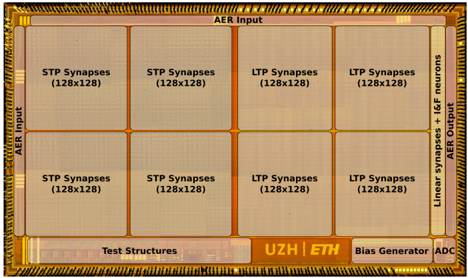
The image is a micrograph or detailed layout diagram of a neuromorphic computing integrated circuit (chip). It shows the physical floorplan of the silicon die, divided into distinct functional blocks and support structures. The design is organized around a central 2x4 grid of synaptic crossbar arrays, with peripheral circuits for input/output, bias generation, and testing.
### Components/Axes
The diagram is a top-down view of the chip die. All text labels are in English.
**Main Grid (Central 2x4 Array):**
* **Top Row (Left to Right):**
1. `STP Synapses (128x128)`
2. `STP Synapses (128x128)`
3. `LTP Synapses (128x128)`
4. `LTP Synapses (128x128)`
* **Bottom Row (Left to Right):**
1. `STP Synapses (128x128)`
2. `STP Synapses (128x128)`
3. `LTP Synapses (128x128)`
4. `LTP Synapses (128x128)`
**Peripheral Labels & Structures:**
* **Top Edge (Center):** `AER Input`
* **Left Edge (Vertical):** `AER Input`
* **Right Edge (Vertical, Top Section):** `Linear Synapses / IF Neurons`
* **Right Edge (Vertical, Bottom Section):** `AER Output`
* **Bottom Edge (Left to Right):**
1. `Test Structures`
2. `UZH | ETH` (within a distinct rectangular block)
3. `Bias Generator`
4. `ADC`
### Detailed Analysis
The chip's core is composed of eight identical-sized synaptic blocks arranged in a symmetrical 2x4 grid. Each block is labeled as a 128x128 crossbar array, indicating a matrix of 128 rows and 128 columns of synaptic connections.
* **Synapse Types:** The grid is divided into two functional types:
* **STP Synapses:** Four blocks (the two leftmost columns) are dedicated to Short-Term Plasticity synapses.
* **LTP Synapses:** Four blocks (the two rightmost columns) are dedicated to Long-Term Plasticity synapses.
* **Signal Flow:** The labeling suggests a data flow from the `AER Input` (top and left) into the synaptic core. Processed signals likely move to the `Linear Synapses / IF Neurons` block on the right, which performs further processing before sending output events via the `AER Output`.
* **Support Circuits:** The bottom strip contains essential auxiliary circuits:
* `Test Structures`: For manufacturing validation and characterization.
* `UZH | ETH`: Logos indicating the design institutions (University of Zurich and ETH Zurich).
* `Bias Generator`: Provides reference voltages/currents for analog circuits.
* `ADC`: Analog-to-Digital Converter, likely for interfacing with external digital systems.
### Key Observations
1. **Symmetry and Modularity:** The design is highly modular and symmetrical, with identical STP and LTP blocks. This suggests a scalable architecture where capacity can be increased by adding more blocks.
2. **Clear Functional Segregation:** There is a strict physical separation between short-term and long-term plasticity resources, which may be for optimizing performance or power for different computational tasks.
3. **Dedicated Neuron Block:** The `Linear Synapses / IF Neurons` block is separate from the main plasticity arrays, indicating a dedicated stage for neuronal integration and linear transformation of synaptic currents.
4. **Institutional Collaboration:** The prominent `UZH | ETH` block highlights this as a research chip from these Swiss institutions.
### Interpretation
This die photo reveals the architecture of a specialized neuromorphic processor designed for event-driven, brain-inspired computation. The core innovation appears to be the large-scale integration of both short-term and long-term synaptic plasticity mechanisms within a single chip, organized into distinct, addressable memory banks.
The use of **AER (Address Event Representation)** for both input and output confirms an asynchronous, event-based communication protocol, which is energy-efficient for sparse data. The 128x128 crossbar arrays represent a significant density of analog synaptic connections, aiming to mimic the parallel connectivity of biological neural networks.
The separation of STP and LTP blocks is particularly noteworthy. It implies the chip can dynamically allocate resources for different timescales of learning and memory—STP for transient, working-memory-like functions, and LTP for more permanent memory formation. This could enable complex, multi-timescale learning algorithms directly in hardware.
The presence of `Linear Synapses` alongside `IF (Integrate-and-Fire) Neurons` suggests the computational model goes beyond simple spiking, incorporating linear transformations which are crucial for many neural network operations. The integrated `ADC` and `Bias Generator` point to a mixed-signal design, where computation happens in the analog domain but interfaces with the digital world.
In summary, this is a research-grade neuromorphic chip designed to explore large-scale, on-chip learning with biologically plausible plasticity rules, likely targeting applications in real-time sensory processing, robotics, or adaptive learning systems.