## Chart: RESET: CMO defect depletion
### Overview
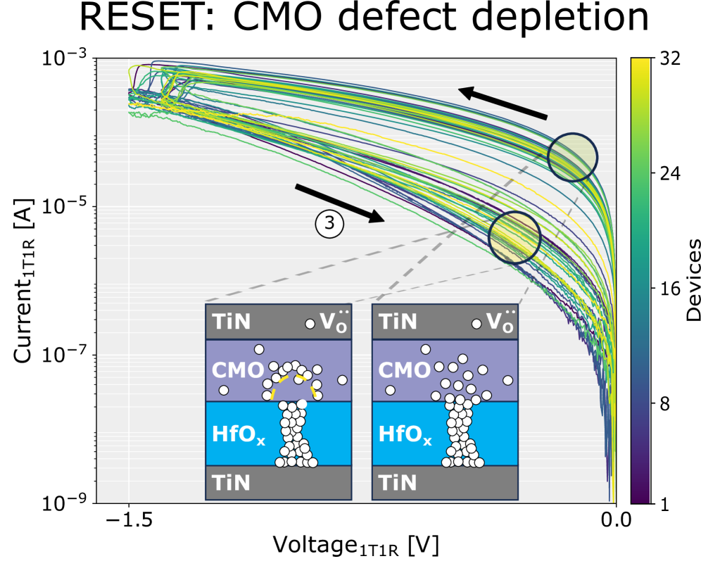
The image presents a chart illustrating the relationship between current (Current<sub>1T1R</sub>) and voltage (Voltage<sub>1T1R</sub>) during a reset process, specifically focusing on CMO defect depletion. The chart displays numerous data curves, with a color gradient representing the density of devices. Below the chart are two diagrams illustrating the device structure before and after defect depletion.
### Components/Axes
* **Title:** RESET: CMO defect depletion (Top-center)
* **X-axis:** Voltage<sub>1T1R</sub> [V] (Bottom-center), ranging from approximately -1.5 to 0.0.
* **Y-axis:** Current<sub>1T1R</sub> [A] (Left-center), on a logarithmic scale ranging from 10<sup>-9</sup> to 10<sup>-3</sup>.
* **Colorbar/Legend:** Located on the right side of the chart, representing the number of devices. The color gradient ranges from dark purple (1 device) to light green (32 devices).
* **Data Series:** Numerous curves representing individual device responses.
* **Annotations:** Two circles with arrows indicating trends. A number "3" is also present with an arrow.
* **Diagrams:** Two schematic diagrams illustrating the device structure before and after defect depletion.
### Detailed Analysis or Content Details
The chart displays a large number of curves, each representing the current-voltage characteristics of a single device. The curves generally show a decreasing current as voltage increases from negative to positive values. The color of each curve corresponds to the density of devices exhibiting similar behavior, as indicated by the colorbar.
**Trend Analysis:**
* **Overall Trend:** The majority of curves exhibit a steep decrease in current as the voltage approaches 0.0 V.
* **High-Density Region:** The region around Voltage<sub>1T1R</sub> = 0.0 V and Current<sub>1T1R</sub> = 10<sup>-7</sup> A to 10<sup>-6</sup> A shows a high density of devices (green color).
* **Low-Density Region:** The region around Voltage<sub>1T1R</sub> = -1.5 V and Current<sub>1T1R</sub> = 10<sup>-3</sup> A shows a low density of devices (dark purple color).
* **Arrow 1 (Top-Left):** Points to a region of curves that initially show a relatively high current at negative voltages, then decrease rapidly as voltage approaches 0.
* **Arrow 2 (Bottom-Right):** Points to the region where most curves converge, indicating a common reset behavior.
* **Annotation "3":** Points to a region of curves that exhibit a more gradual decrease in current.
**Diagram Analysis:**
* **Left Diagram (Before Depletion):** Shows a layered structure: TiN / HfO<sub>x</sub> / CMO / HfO<sub>x</sub> / TiN. The CMO layer contains several "V<sub>O</sub>" defects (oxygen vacancies) represented as white circles.
* **Right Diagram (After Depletion):** Shows a similar layered structure, but the CMO layer has significantly fewer V<sub>O</sub> defects. The defects appear to have been reduced or eliminated.
### Key Observations
* The chart demonstrates a clear correlation between voltage and current during the reset process.
* The color gradient indicates that the reset behavior is relatively consistent across a large number of devices.
* The diagrams suggest that the reset process involves the depletion of oxygen vacancies (V<sub>O</sub>) in the CMO layer.
* The curves show a wide range of current values at a given voltage, indicating some variability in device characteristics.
* The number "3" annotation suggests a subset of devices exhibiting a different reset behavior.
### Interpretation
The data suggests that the reset process in these devices is driven by the depletion of oxygen vacancies in the CMO layer. Applying a voltage causes the defects to be eliminated, leading to a decrease in current. The color gradient on the chart indicates that this process is relatively consistent across the device population. The diagrams visually represent this defect depletion mechanism. The variability in the curves suggests that the initial distribution of defects and other device parameters may influence the reset behavior. The annotation "3" could indicate devices with a different defect structure or a different reset mechanism. The chart provides valuable insights into the physics of the reset process and could be used to optimize device performance. The logarithmic scale on the Y-axis is crucial for visualizing the wide range of current values.