## State Diagram and Memory Allocation
### Overview
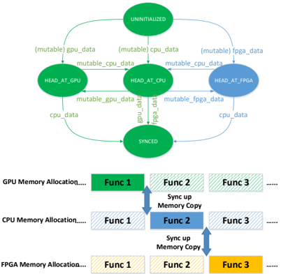
The image presents a state diagram illustrating data handling between GPU, CPU, and FPGA, coupled with a memory allocation scheme for each. The state diagram shows transitions between states like UNINITIALIZED, HEAD_AT_GPU, HEAD_AT_CPU, HEAD_AT_FPGA, and SYNCED, driven by data transfers. The memory allocation section depicts how functions are allocated in GPU, CPU, and FPGA memory, with synchronization mechanisms between them.
### Components/Axes
**State Diagram Components:**
* **States:** UNINITIALIZED, HEAD_AT_GPU, HEAD_AT_CPU, HEAD_AT_FPGA, SYNCED (represented as green or blue ovals).
* **Transitions:** Arrows indicating data flow between states, labeled with data types (e.g., "(mutable) gpu\_data", "cpu\_data").
**Memory Allocation Components:**
* **Memory Types:** GPU Memory Allocation, CPU Memory Allocation, FPGA Memory Allocation.
* **Functions:** Func 1, Func 2, Func 3 (represented as colored blocks).
* **Synchronization:** Arrows indicating "Sync up Memory Copy" between CPU and GPU, and CPU and FPGA.
### Detailed Analysis
**State Diagram:**
* **UNINITIALIZED:** The initial state. Transitions to HEAD_AT_GPU, HEAD_AT_CPU, and HEAD_AT_FPGA via "(mutable) gpu\_data", "(mutable) cpu\_data", and "(mutable) fpga\_data" respectively.
* **HEAD_AT_GPU:** Transitions to HEAD_AT_CPU via "mutable\_cpu\_data", to SYNCED via "cpu\_data", and back to itself.
* **HEAD_AT_CPU:** Transitions to HEAD_AT_GPU via "mutable\_gpu\_data", to SYNCED via "fpga\_data", and to HEAD_AT_FPGA via "mutable\_fpga\_data".
* **HEAD_AT_FPGA:** Transitions to SYNCED via "cpu\_data".
* **SYNCED:** Transitions to HEAD_AT_GPU via "gpu\_data", to HEAD_AT_CPU via "cpu\_data", and to HEAD_AT_FPGA via "fpga\_data".
**Memory Allocation:**
* **GPU Memory Allocation:**
* Func 1: Solid green block.
* Func 2: Green block with diagonal lines.
* Func 3: Green block with diagonal lines.
* **CPU Memory Allocation:**
* Func 1: Blue block with diagonal lines.
* Func 2: Solid blue block.
* Func 3: Blue block with diagonal lines.
* **FPGA Memory Allocation:**
* Func 1: Yellow block with diagonal lines.
* Func 2: Yellow block with diagonal lines.
* Func 3: Solid yellow block.
* **Synchronization:**
* "Sync up Memory Copy" occurs between Func 2 of GPU and CPU.
* "Sync up Memory Copy" occurs between Func 3 of CPU and FPGA.
### Key Observations
* The state diagram illustrates a data management workflow between different processing units.
* The memory allocation section shows a function distribution across GPU, CPU, and FPGA memory spaces.
* Synchronization is explicitly shown between GPU and CPU, and CPU and FPGA, suggesting data consistency requirements.
* HEAD_AT_FPGA is colored blue, while the other states are colored green.
### Interpretation
The diagram describes a heterogeneous computing system where data is processed across GPU, CPU, and FPGA. The state diagram defines the flow of data and the conditions under which data is transferred between these units. The "mutable" keyword suggests that data can be modified during these transitions. The memory allocation scheme indicates that different functions are assigned to different processing units, likely based on their suitability for specific tasks. The synchronization steps are crucial for maintaining data integrity across the different memory spaces, ensuring that the CPU, GPU, and FPGA have consistent views of the data when needed. The color difference of HEAD_AT_FPGA may indicate a different state or configuration.