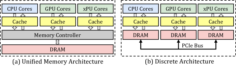
## Diagram: Unified vs. Discrete Memory Architectures
### Overview
The image displays two side-by-side block diagrams comparing computer system memory architectures. The left diagram (a) illustrates a "Unified Memory Architecture," while the right diagram (b) illustrates a "Discrete Architecture." Both diagrams show the hierarchical relationship between processing cores, cache memory, and main memory (DRAM).
### Components/Axes
The diagrams are composed of labeled rectangular blocks connected by arrows indicating data flow or connection paths.
**Diagram (a) - Left Side:**
* **Title/Label:** "(a) Unified Memory Architecture" (located below the diagram).
* **Top Row (Processing Cores):** Three blocks labeled "CPU Cores", "GPU Cores", and "xPU Cores".
* **Second Row (Cache):** Three blocks, each labeled "Cache", positioned directly below each corresponding core block.
* **Third Row (Memory Controller):** A single, wide block labeled "Memory Controller" spanning the width beneath all three cache blocks.
* **Bottom Row (Main Memory):** A single, wide block labeled "DRAM" positioned below the Memory Controller.
* **Connections:**
* Bidirectional arrows connect each "Cores" block to its corresponding "Cache" block.
* Bidirectional arrows connect each "Cache" block to the unified "Memory Controller".
* A bidirectional arrow connects the "Memory Controller" to the single "DRAM" block.
**Diagram (b) - Right Side:**
* **Title/Label:** "(b) Discrete Architecture" (located below the diagram).
* **Top Row (Processing Cores):** Identical to (a): "CPU Cores", "GPU Cores", "xPU Cores".
* **Second Row (Cache):** Identical to (a): Three "Cache" blocks.
* **Third Row (Main Memory):** Three separate blocks labeled "DRAM", each positioned below a corresponding "Cache" block.
* **Connection Bus:** A horizontal line labeled "PCIe Bus" runs below the three DRAM blocks.
* **Connections:**
* Bidirectional arrows connect each "Cores" block to its corresponding "Cache" block.
* Bidirectional arrows connect each "Cache" block directly to its dedicated "DRAM" block below it.
* Single-headed arrows point upward from the "PCIe Bus" line to each of the three "DRAM" blocks.
### Detailed Analysis
The diagrams contrast two fundamental approaches to connecting processors to memory.
* **In the Unified Architecture (a):** All processor types (CPU, GPU, xPU) share a common path to a single pool of memory (DRAM) via a central Memory Controller. This implies a shared, addressable memory space accessible by all cores.
* **In the Discrete Architecture (b):** Each processor type has its own dedicated DRAM module. The "Cache" for each core type connects directly to its private DRAM. The separate DRAM modules are interconnected via a "PCIe Bus," which is a standard high-speed interface for component communication. This implies memory is physically partitioned and explicit data transfer between processor-specific memory pools is required.
### Key Observations
1. **Component Consistency:** Both architectures use the same set of processing core types (CPU, GPU, xPU) and include a cache level for each.
2. **Structural Divergence:** The critical difference lies below the cache level. Diagram (a) converges to a single memory controller and DRAM, while diagram (b) diverges into three separate DRAM blocks.
3. **Interconnect Difference:** The unified architecture uses a proprietary or integrated memory controller bus. The discrete architecture uses the standardized "PCIe Bus" to connect the disparate memory modules.
4. **Spatial Layout:** The diagrams are presented in a direct, comparative layout within dashed bounding boxes, emphasizing their contrasting structures. All text is in English.
### Interpretation
These diagrams visually explain a core trade-off in heterogeneous computing system design.
* **Unified Memory (a)** simplifies software development because programmers can treat memory as a single, shared resource. Data does not need to be explicitly copied between CPU, GPU, and xPU memory spaces. The potential downside is contention for the single memory controller and DRAM bandwidth, which could become a bottleneck if all cores access memory intensively simultaneously.
* **Discrete Memory (b)** offers potentially higher aggregate memory bandwidth because each processor type has its own dedicated DRAM. However, it complicates programming significantly. Data must be explicitly managed and transferred between the CPU's DRAM, GPU's DRAM, and xPU's DRAM over the PCIe bus, adding latency and programming overhead. This architecture is common in traditional systems where accelerators (like discrete GPUs) are add-in cards.
The diagrams effectively communicate that the choice between these architectures involves balancing **programming simplicity and unified addressability** (Unified) against **potential performance isolation and dedicated bandwidth** (Discrete). The presence of "xPU Cores" suggests this is a modern context discussing accelerators beyond just CPUs and GPUs.