\n
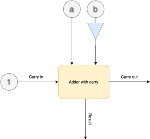
## Diagram: Adder with Carry
### Overview
The image depicts a block diagram illustrating a full adder with a carry input and output. It shows the inputs 'a' and 'b', a carry-in signal, and the resulting output 'Result' along with a carry-out signal. The diagram represents a fundamental building block in digital logic circuits.
### Components/Axes
The diagram consists of the following components:
* **Inputs:** 'a' and 'b' - represented by circles at the top of the diagram.
* **Adder Block:** A yellow rectangle labeled "Adder with carry".
* **Carry-in:** An arrow labeled "Carry in" originating from a circle labeled "1" on the left side.
* **Carry-out:** An arrow labeled "Carry out" extending from the right side of the adder block.
* **Result:** An arrow labeled "Result" extending downwards from the adder block.
* **Combinational Logic:** A blue triangle connecting inputs 'a' and 'b' to the adder block.
### Detailed Analysis
The diagram illustrates the flow of data through a full adder.
1. **Inputs 'a' and 'b':** These are the two bits to be added. They are connected to the adder block via a blue triangle, indicating a combinational logic operation.
2. **Carry-in:** A carry-in signal, originating from a circle labeled "1", is fed into the adder block. This represents a carry bit from a previous addition stage.
3. **Adder with Carry:** The core component, which performs the addition of 'a', 'b', and the carry-in.
4. **Result:** The sum of the addition is output as the 'Result'.
5. **Carry-out:** If the sum exceeds one bit, a carry-out signal is generated and output.
The diagram does not provide specific numerical values or timing information. It is a conceptual representation of the adder's functionality.
### Key Observations
* The diagram clearly shows the adder as a combinational logic block, taking three inputs and producing two outputs.
* The carry-in signal is explicitly shown, indicating a full adder rather than a half adder.
* The diagram is simplified and does not show the internal logic gates within the adder block.
### Interpretation
This diagram represents a fundamental building block in digital systems – the full adder. It demonstrates how binary numbers can be added together, taking into account carry bits from previous stages. The diagram is a high-level representation, focusing on the inputs, outputs, and overall functionality of the adder. It is a crucial component in arithmetic logic units (ALUs) and other digital circuits that perform arithmetic operations. The circle labeled "1" for the carry-in suggests this adder might be part of a larger system where the carry-in is a constant value, or the beginning of a multi-bit addition. The use of arrows indicates the direction of signal flow, and the distinct shapes (circles, rectangles, triangles) help to visually differentiate the components and their roles.