## Block Diagram: Binary Adder Circuit
### Overview
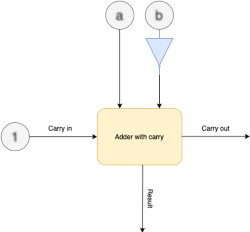
The diagram illustrates a simplified digital adder circuit with two input bits (`a` and `b`), a carry-in input (`1`), and outputs for carry-out and result. The adder block processes the inputs to produce a binary sum and carry propagation.
### Components/Axes
- **Inputs**:
- `a` (top-left): Binary input bit.
- `b` (top-right): Binary input bit.
- `1` (bottom-left): Constant carry-in input (value = 1).
- **Adder Block**: Central yellow rectangle labeled "Adder with carry."
- **Outputs**:
- `Carry out` (right): Propagated carry signal.
- `Result` (bottom): Sum of `a`, `b`, and carry-in.
### Detailed Analysis
- **Flow Direction**:
- `a` and `b` flow into the adder block from the top.
- The constant `1` (carry-in) enters from the left.
- `Carry out` exits to the right.
- `Result` exits downward.
- **Key Connections**:
- The `1` input is directly connected to the adder’s carry-in terminal, ensuring the circuit performs addition with a predefined carry.
- The adder block’s output splits into two paths: `Carry out` (right) and `Result` (bottom).
### Key Observations
- The diagram lacks numerical values or explicit logic gates (e.g., XOR, AND), focusing instead on high-level signal flow.
- The constant `1` input suggests the adder is configured for a specific operation (e.g., incrementing a value by 1).
- No feedback loops or additional components (e.g., registers, multiplexers) are shown.
### Interpretation
This diagram represents a **1-bit full adder** with a fixed carry-in of `1`. The circuit adds two binary digits (`a` and `b`) along with the carry-in, producing a sum (`Result`) and a carry-out for chaining with higher-order bits.
- **Functionality**:
- If `a = 0` and `b = 0`, `Result = 1` (0 + 0 + 1 = 1, no carry-out).
- If `a = 1` and `b = 1`, `Result = 1` with `Carry out = 1` (1 + 1 + 1 = 3 in binary: `11`).
- **Design Implications**:
- The absence of variable carry-in inputs limits flexibility but simplifies the circuit for specific use cases (e.g., fixed-increment operations).
- The split output paths indicate modularity, allowing integration into larger multi-bit adder architectures.
No numerical data or trends are present; the diagram focuses on structural relationships and signal propagation.