TECHNICAL ASSET FINGERPRINT
aa6d4ad699d62ee0d3966ca5
Click to view fullscreen
Press ESC or click to close
FOUND IN PAPERS
EXPERT: gemini-2.0-flash VERSION 1
RUNTIME: nugit/gemini/gemini-2.0-flash
INTEL_VERIFIED
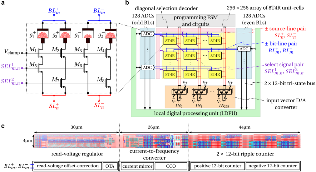
## Circuit Diagram: 8T4R Unit-Cell Array and Peripheral Circuits
### Overview
The image presents a detailed circuit diagram of an 8T4R unit-cell array along with its peripheral circuits. It is divided into three main sections: (a) a schematic of the unit cell, (b) a block diagram of the array and its associated digital processing unit, and (c) a layout view of the key circuit blocks.
### Components/Axes
**Section a:**
* **Labels:**
* `BL⁺m`, `BL⁻m`: Bit-line pair (top, blue)
* `g₁⁺`, `g₂⁺`, `g₁⁻`, `g₂⁻`: Gate labels within the unit cell
* `Vclamp`: Clamp voltage (left)
* `SEL¹m,n`, `SEL²m,n`: Select signal pair (left, purple)
* `SL⁺n`, `SL⁻n`: Source-line pair (bottom, red)
* `M₁` to `M₈`: Transistor labels
**Section b:**
* **Labels:**
* "diagonal selection decoder" (top, gray box)
* "programming FSM and circuits" (top, gray box)
* "256 x 256 array of 8T4R unit-cells" (top, right)
* "128 ADCs (odd BLs)" (left, blue box)
* "128 ADCs (even BLs)" (right, blue box)
* "ADC": Analog-to-digital converter
* "8T4R": Unit cell block
* `V+`, `V-`: Voltage references
* `IN₀`, `IN₁`, ..., `IN₂₅₅`: Input nodes
* "local digital processing unit (LDPU)" (bottom, green box)
* "2 x 12-bit tri-state bus" (right, purple dotted line)
* "input vector D/A converter" (right, purple dotted line)
* **Legend (right side):**
* Red dotted line: "± source-line pair `SL⁺n`, `SL⁻n`"
* Blue dotted line: "± bit-line pair `BL⁺m`, `BL⁻m`"
* Purple dotted line: "select signal pair `SEL¹m,n`, `SEL²m,n`"
**Section c:**
* **Dimensions:**
* Read-voltage regulator: 30µm (width), 4µm (height)
* Current-to-frequency converter: 26µm (width), 4µm (height)
* 2 x 12-bit ripple counter: 44µm (width), 4µm (height)
* **Functional Blocks:**
* read-voltage regulator
* current-to-frequency converter
* 2 x 12-bit ripple counter
* **Sub-Blocks:**
* read-voltage offset-correction
* OTA (Operational Transconductance Amplifier)
* current mirror
* CCO (Current-Controlled Oscillator)
* positive 12-bit counter
* negative 12-bit counter
### Detailed Analysis
**Section a:**
* The circuit shows a memory cell with transistors `M₁` to `M₈`.
* The bit-lines `BL⁺m` and `BL⁻m` are connected to the gates of transistors `M₁`, `M₂`, `M₃`, and `M₄`.
* The select lines `SEL¹m,n` and `SEL²m,n` control transistors `M₅`, `M₆`, `M₇`, and `M₈`.
* The source lines `SL⁺n` and `SL⁻n` are connected to the sources of transistors `M₇` and `M₈`.
**Section b:**
* A 256x256 array of 8T4R unit cells is shown.
* 128 ADCs are used for both odd and even bit-lines.
* A diagonal selection decoder and programming FSM control the array.
* The local digital processing unit (LDPU) contains input vector D/A converters.
**Section c:**
* The layout shows the physical dimensions of the read-voltage regulator, current-to-frequency converter, and 2 x 12-bit ripple counter.
* The read-voltage regulator includes read-voltage offset-correction and an OTA.
* The current-to-frequency converter includes a current mirror and a CCO.
* The 2 x 12-bit ripple counter includes positive and negative 12-bit counters.
### Key Observations
* The diagram illustrates the architecture of a memory system based on 8T4R unit cells.
* The system includes analog-to-digital conversion, digital processing, and voltage regulation.
* The layout provides information about the physical dimensions and organization of the circuit blocks.
### Interpretation
The image provides a comprehensive overview of a memory system design, highlighting the integration of analog and digital components. The 8T4R unit cell array is controlled by a diagonal selection decoder and programming FSM, enabling read and write operations. The local digital processing unit (LDPU) performs signal processing and data conversion. The layout view provides insights into the physical implementation of the circuit, showing the arrangement of functional blocks and their dimensions. This level of detail is crucial for understanding the performance and characteristics of the memory system.
DECODING INTELLIGENCE...
EXPERT: gemma-3-27b-it-free VERSION 1
RUNTIME: google-free/gemma-3-27b-it
INTEL_VERIFIED
\n
## Diagram: Image Sensor Architecture
### Overview
The image presents a schematic of an image sensor architecture, broken down into three sections: a single-cell circuit (a), an array architecture (b), and layout views of key components (c). The diagram details the circuitry for a pixel, the organization of pixels into an array with associated digital processing, and the physical layout of certain modules.
### Components/Axes
**Section a (Single-Cell Circuit):**
* Labels: `BLm+`, `BLm-`, `SLn+`, `SLn-`, `Vclamp`, `SELm,n`, `SELm,n`, `M1`, `M2`, `M3`, `M4`, `M5`, `M6`, `M7`, `M8`, `g1`, `g2`.
* Components: Transistors (labeled M1-M8), Capacitors (implied by the circuit connections), Voltage source (`Vclamp`).
**Section b (Array Architecture):**
* Labels: "256 x 256 array of 8T4R unit-cells", "128 ADCs (odd BLs)", "128 ADCs (even BLs)", "diagonal selection decoder", "programming FSM and circuits", "local digital processing unit (LDPU)", "source-line pair SLn+ SLn-", "+ bit-line pair BLm+ BLm-", "select signal pair SELm,n SELm,n", "2 x 12-bit tri-state bus", "input vector D/A converter".
* Components: Array of unit cells, Analog-to-Digital Converters (ADCs), Finite State Machine (FSM), Digital Processing Unit (LDPU), Buses, D/A converter.
**Section c (Layout Views):**
* Labels: "30µm", "26µm", "44µm", "4µm", "read-voltage regulator", "read-voltage offset-correction", "OTA", "current-to-frequency converter", "current mirror", "CCO", "positive 12-bit counter", "negative 12-bit counter".
* Components: Layout representations of read-voltage regulator, current-to-frequency converter, and counters. Dimensions are provided in micrometers (µm).
### Detailed Analysis or Content Details
**Section a (Single-Cell Circuit):**
The circuit appears to be a 4T/8T pixel structure. Transistors M1 and M2 form a differential pair, with M3 and M4 acting as current sources. M5-M8 are switching transistors controlled by the select signals `SELm,n`. The `Vclamp` provides a reference voltage. The bitlines `BLm+` and `BLm-` are connected to the differential pair, and the sourcelines `SLn+` and `SLn-` provide the input signal path.
**Section b (Array Architecture):**
The diagram shows a 256x256 array of unit cells. The bitlines are divided into odd and even sets, each connected to 128 ADCs. A diagonal selection decoder and programming FSM control the pixel selection and readout. The LDPU processes the digital data from the ADCs. The output is a 2x12-bit tri-state bus connected to an input vector D/A converter.
**Section c (Layout Views):**
* **30µm View (Read-Voltage Regulator):** Shows a layout of a read-voltage regulator, with dimensions approximately 30µm x 4µm. The layout includes components labeled "read-voltage offset-correction" and "OTA".
* **26µm View (Current-to-Frequency Converter):** Displays a layout of a current-to-frequency converter, approximately 26µm x 4µm. It includes a "current mirror" and "CCO" (Current Controlled Oscillator).
* **44µm View (Counters):** Shows a layout of a 2x12-bit ripple counter, approximately 44µm x 4µm. It contains a "positive 12-bit counter" and a "negative 12-bit counter".
### Key Observations
* The architecture utilizes a large array of unit cells (256x256) to achieve high resolution.
* The use of ADCs and a LDPU indicates on-chip digital processing for improved performance and reduced data bandwidth.
* The layout views provide insight into the physical size and complexity of the key components.
* The pixel circuit appears to be a relatively complex design, likely optimized for low noise and high sensitivity.
### Interpretation
The diagram illustrates a sophisticated image sensor architecture designed for high-resolution imaging with on-chip processing capabilities. The 8T/4R pixel structure suggests a focus on minimizing noise and maximizing dynamic range. The inclusion of a LDPU and ADCs indicates a move towards "smart" sensors that can perform some level of image processing before outputting the data. The layout views demonstrate the feasibility of integrating these complex circuits onto a single chip. The separation of bitlines into odd and even sets, coupled with dedicated ADCs, likely enables parallel readout and faster frame rates. The use of a diagonal selection decoder suggests a strategy for reducing power consumption and improving signal integrity. The inclusion of both positive and negative counters suggests a design that can handle both positive and negative signals, potentially for HDR (High Dynamic Range) imaging. The overall design appears to be a well-integrated system optimized for performance, power efficiency, and functionality.
DECODING INTELLIGENCE...
EXPERT: healer-alpha-free VERSION 1
RUNTIME: free/openrouter/healer-alpha
INTEL_VERIFIED
## Technical Diagram Composite: 8T4R Unit-Cell and Array Architecture
### Overview
The image is a composite of three technical diagrams (labeled a, b, and c) detailing the circuit design, system architecture, and physical layout of a memory/processing array based on an 8T4R (8-transistor, 4-resistor) unit-cell. The diagrams progress from a transistor-level schematic to a system-level block diagram and finally to a physical layout view.
### Components/Axes
The image contains three distinct panels:
* **Panel a:** A circuit schematic of a single 8T4R unit-cell.
* **Panel b:** A block diagram of a 256x256 array of these unit-cells and its supporting circuitry.
* **Panel c:** A physical layout diagram of a key circuit block with dimensional annotations.
### Detailed Analysis
#### **Panel a: 8T4R Unit-Cell Schematic**
* **Type:** Circuit Schematic.
* **Components & Labels:**
* **Resistive Elements:** Four memristor-like devices labeled `g₁⁺`, `g₂⁺`, `g₁⁻`, `g₂⁻`. They are depicted as red rectangles with a wavy internal pattern.
* **Transistors:** Eight NMOS transistors labeled `M₁` through `M₈`.
* **Voltage/Signal Lines:**
* `Vclamp`: A clamping voltage input connected to the gates of `M₁` and `M₃`.
* `SEL¹ₘ,ₙ` and `SEL²ₘ,ₙ`: Select signal lines (purple) connected to the gates of `M₅`/`M₆` and `M₇`/`M₈` respectively.
* `BL⁺ₘ` and `BL⁻ₘ`: Positive and negative bit-line pairs (blue) connected to the top of the resistive elements.
* `SL⁺ₙ` and `SL⁻ₙ`: Positive and negative source-line pairs (red) connected to the bottom of the transistor network.
* **Structure:** The circuit is arranged in two symmetrical vertical branches. The left branch contains `g₁⁺`, `g₂⁺`, `M₁`, `M₂`, `M₅`, `M₇`. The right branch contains `g₁⁻`, `g₂⁻`, `M₃`, `M₄`, `M₆`, `M₈`. The `Vclamp` and `SEL` signals control the connection of the resistive elements to the source lines.
#### **Panel b: 256x256 Array and System Architecture**
* **Type:** System Block Diagram.
* **Components & Labels (Spatially Grounded):**
* **Top Region:**
* `diagonal selection decoder` (text, top-left).
* `programming FSM and circuits` (text, top-center, within a grey box).
* **Main Array Region (Center):**
* A grid labeled `256 x 256 array of 8T4R unit-cells` (text, top-right).
* The grid is composed of yellow squares, each labeled `8T4R`.
* **Left Side:** A column of blocks labeled `128 ADCs (odd BLs)`.
* **Right Side:** A column of blocks labeled `128 ADCs (even BLs)`.
* **Bottom Region:**
* A large green block labeled `local digital processing unit (LDPU)`.
* Within the LDPU: Three blocks labeled `V+`, `V-`, and `IN₀`, `IN₁`, ..., `IN₂₅₅`, connected to a `2 x 12-bit tri-state bus` and an `input vector D/A converter`.
* **Legend (Right Side, Spatially Grounded):**
* **Red Text/Lines:** `± source-line pair SL⁺ₙ, SL⁻ₙ`. These lines run vertically through the array.
* **Blue Text/Lines:** `± bit-line pair BL⁺ₘ, BL⁻ₘ`. These lines run horizontally through the array.
* **Purple Text/Lines:** `select signal pair SEL¹ₘ,ₙ, SEL²ₘ,ₙ`. These lines run diagonally from the top-left decoder.
* **Flow & Relationships:** The diagram shows a hierarchical structure. The diagonal decoder and programming FSM control the 256x256 core array. The array is read by 128 ADCs on each side (for odd and even bit-lines). The processed data is handled by the LDPU at the bottom, which includes digital-to-analog conversion for input vectors.
#### **Panel c: Physical Layout Diagram**
* **Type:** Layout Diagram with Dimensions.
* **Components & Labels:**
* **Top Dimension Line:** Spans the entire width with three segments: `30µm`, `26µm`, `44µm`.
* **Left Dimension:** `4µm` indicating the height of the layout.
* **Main Layout Blocks (from left to right):**
* `read-voltage regulator` (under the 30µm segment).
* `current-to-frequency converter` (under the 26µm segment).
* `2 x 12-bit ripple counter` (under the 44µm segment).
* **Sub-Block Diagram (Bottom):** A simplified block diagram corresponding to the layout above.
* Input: `BL⁺ₘ, BL⁻ₘ`.
* Blocks: `read-voltage offset-correction`, `OTA`, `current mirror`, `CCO`, `positive 12-bit counter`, `negative 12-bit counter`.
* **Spatial Grounding:** The layout is a long, thin rectangle (4µm tall). The functional blocks are arranged linearly from left to right, matching the dimensional segments above them.
### Key Observations
1. **Symmetry and Differential Design:** The unit-cell (a) and the array bit/source lines (b) use fully differential signaling (`+`/`-` pairs), which is common for noise immunity in sensitive memory/processing arrays.
2. **Hierarchical Integration:** The diagrams show a clear hierarchy from device (a) to array subsystem (b) to a specific circuit's physical implementation (c).
3. **Mixed-Signal Design:** The system integrates analog components (memristors, ADCs, OTAs, regulators) with digital control (FSM, decoders, counters, LDPU).
4. **Scalability:** The 256x256 array specification indicates a focus on creating a scalable core for computation-in-memory or analog processing applications.
5. **Precision Layout:** The 4µm height and specific length allocations (30µm, 26µm, 44µm) in panel (c) highlight the careful physical design required for analog blocks like the read-voltage regulator and current-to-frequency converter.
### Interpretation
This set of diagrams describes a complete compute-in-memory or analog signal processing subsystem. The **8T4R cell** is the fundamental storage/processing element, likely using its resistive states (`g`) to perform analog multiplication or synaptic weighting. The **256x256 array** forms a crossbar where these operations can be performed in parallel on input vectors (provided by the LDPU's D/A converter). The **ADCs** convert the analog results (e.g., currents summed on the bit-lines) back to digital for further processing by the LDPU.
The **layout in panel (c)** focuses on a critical analog front-end circuit—the read-voltage regulator and current-to-frequency converter. This block is essential for accurately reading the state of the unit-cells and converting that analog current into a digital frequency count (via the ripple counters), which is a common technique for high-precision, low-power analog-to-digital conversion in such systems.
**Overall Purpose:** The system is designed for efficient, parallel analog computation, potentially for neural network inference, signal processing, or other matrix-vector multiplication tasks, where the memory array itself performs the computation, reducing data movement bottlenecks. The detailed layout underscores the importance of analog circuit precision in realizing the theoretical benefits of the architecture.
DECODING INTELLIGENCE...
EXPERT: nemotron-free VERSION 2
RUNTIME: free/nvidia/nemotron-nano-12b-v2-vl:free
INTEL_VERIFIED
## Technical Circuit Diagram: Memory System Architecture
### Overview
The image depicts a complex memory system architecture divided into three sections:
- **a**: Memory cell array with bit lines (BL), select lines (SL), and access transistors.
- **b**: System-level block diagram showing analog-to-digital conversion (ADC), programming logic, and digital processing.
- **c**: Signal processing chain including voltage regulation, current-to-frequency conversion, and digital counting.
### Components/Axes
#### Part a (Memory Cell Array)
- **Labels**:
- `BL_m+`/`BL_m-`: Bit lines (positive/negative).
- `SL_n+`/`SL_n-`: Select lines (positive/negative).
- `M1–M8`: Memory cells (likely 8T4R unit-cells).
- `g1–g2`: Access transistors.
- `Vclamp`: Clamp voltage source.
- `SEL1_m,n`/`SEL2_m,n`: Select signal pairs for row/column addressing.
- **Spatial Layout**:
- Bit lines (`BL_m+`, `BL_m-`) at the top.
- Memory cells (`M1–M8`) in the middle.
- Select lines (`SL_n+`, `SL_n-`) at the bottom.
#### Part b (System-Level Architecture)
- **Labels**:
- `8T4R unit-cells`: Memory cells with 8 transistors and 4 resistors.
- `128 ADCs`: Analog-to-digital converters for odd/even bit lines.
- `Programming FSM`: Finite state machine for write operations.
- `LDPU`: Local digital processing unit with ripple counters.
- `Input vector D/A converter`: Converts digital inputs to analog signals.
- **Flow**:
- Data flows from ADCs → Programming FSM → LDPU.
- Select signal pairs (`SEL1_m,n`, `SEL2_m,n`) control row/column access.
#### Part c (Signal Processing Chain)
- **Labels**:
- `Read-voltage regulator`: Stabilizes read voltage.
- `Current-to-frequency converter`: Converts current to frequency (CCO).
- `2x12-bit ripple counter`: Digitizes frequency into positive/negative counts.
- **Dimensions**:
- Read-voltage regulator: 30µm.
- Current-to-frequency converter: 26µm.
- Ripple counter: 44µm.
### Detailed Analysis
- **Part a**:
- The memory array uses cross-coupled transistors (`M1–M8`) to store data.
- Bit lines (`BL_m+`, `BL_m-`) and select lines (`SL_n+`, `SL_n-`) enable row/column addressing.
- `Vclamp` ensures stable voltage during read/write operations.
- **Part b**:
- The 256x256 array of 8T4R cells suggests high-density non-volatile memory (e.g., MRAM).
- Odd/even bit lines are processed by separate ADCs (128 ADCs total).
- The LDPU includes a 2x12-bit ripple counter for digital signal processing.
- **Part c**:
- The read-voltage regulator ensures consistent voltage for accurate ADC conversion.
- The current-to-frequency converter (CCO) digitizes analog current signals.
- Ripple counters handle overflow/underflow for 12-bit resolution.
### Key Observations
1. **Hybrid Analog-Digital Design**: Combines analog memory access (BL/SL) with digital processing (LDPU).
2. **High-Density Storage**: 256x256 array of 8T4R cells implies ~65,536 memory cells.
3. **Signal Integrity**: Clamp voltage and offset correction (OTA) mitigate noise in read operations.
4. **Scalability**: Modular components (e.g., 128 ADCs) allow expansion for larger memory arrays.
### Interpretation
This architecture represents a **high-density, low-power memory system** optimized for analog-digital hybrid processing. The use of 8T4R cells suggests non-volatile storage (e.g., MRAM), while the LDPU enables on-chip computation, reducing data transfer latency. The current-to-frequency conversion and ripple counters indicate a focus on energy-efficient digital signal processing, critical for applications like AI accelerators or edge computing. The modular design (e.g., separate ADCs for odd/even BLs) highlights scalability and fault tolerance.
DECODING INTELLIGENCE...