## Circuit Diagram: 8T4R Unit-Cell Array and Peripheral Circuits
### Overview
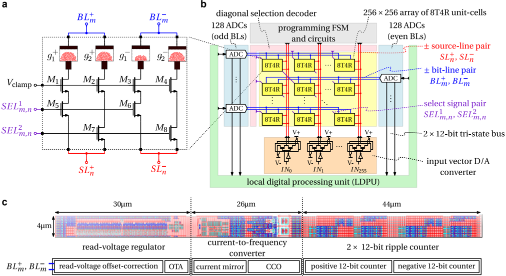
The image presents a detailed circuit diagram of an 8T4R unit-cell array along with its peripheral circuits. It is divided into three main sections: (a) a schematic of the unit cell, (b) a block diagram of the array and its associated digital processing unit, and (c) a layout view of the key circuit blocks.
### Components/Axes
**Section a:**
* **Labels:**
* `BL⁺m`, `BL⁻m`: Bit-line pair (top, blue)
* `g₁⁺`, `g₂⁺`, `g₁⁻`, `g₂⁻`: Gate labels within the unit cell
* `Vclamp`: Clamp voltage (left)
* `SEL¹m,n`, `SEL²m,n`: Select signal pair (left, purple)
* `SL⁺n`, `SL⁻n`: Source-line pair (bottom, red)
* `M₁` to `M₈`: Transistor labels
**Section b:**
* **Labels:**
* "diagonal selection decoder" (top, gray box)
* "programming FSM and circuits" (top, gray box)
* "256 x 256 array of 8T4R unit-cells" (top, right)
* "128 ADCs (odd BLs)" (left, blue box)
* "128 ADCs (even BLs)" (right, blue box)
* "ADC": Analog-to-digital converter
* "8T4R": Unit cell block
* `V+`, `V-`: Voltage references
* `IN₀`, `IN₁`, ..., `IN₂₅₅`: Input nodes
* "local digital processing unit (LDPU)" (bottom, green box)
* "2 x 12-bit tri-state bus" (right, purple dotted line)
* "input vector D/A converter" (right, purple dotted line)
* **Legend (right side):**
* Red dotted line: "± source-line pair `SL⁺n`, `SL⁻n`"
* Blue dotted line: "± bit-line pair `BL⁺m`, `BL⁻m`"
* Purple dotted line: "select signal pair `SEL¹m,n`, `SEL²m,n`"
**Section c:**
* **Dimensions:**
* Read-voltage regulator: 30µm (width), 4µm (height)
* Current-to-frequency converter: 26µm (width), 4µm (height)
* 2 x 12-bit ripple counter: 44µm (width), 4µm (height)
* **Functional Blocks:**
* read-voltage regulator
* current-to-frequency converter
* 2 x 12-bit ripple counter
* **Sub-Blocks:**
* read-voltage offset-correction
* OTA (Operational Transconductance Amplifier)
* current mirror
* CCO (Current-Controlled Oscillator)
* positive 12-bit counter
* negative 12-bit counter
### Detailed Analysis
**Section a:**
* The circuit shows a memory cell with transistors `M₁` to `M₈`.
* The bit-lines `BL⁺m` and `BL⁻m` are connected to the gates of transistors `M₁`, `M₂`, `M₃`, and `M₄`.
* The select lines `SEL¹m,n` and `SEL²m,n` control transistors `M₅`, `M₆`, `M₇`, and `M₈`.
* The source lines `SL⁺n` and `SL⁻n` are connected to the sources of transistors `M₇` and `M₈`.
**Section b:**
* A 256x256 array of 8T4R unit cells is shown.
* 128 ADCs are used for both odd and even bit-lines.
* A diagonal selection decoder and programming FSM control the array.
* The local digital processing unit (LDPU) contains input vector D/A converters.
**Section c:**
* The layout shows the physical dimensions of the read-voltage regulator, current-to-frequency converter, and 2 x 12-bit ripple counter.
* The read-voltage regulator includes read-voltage offset-correction and an OTA.
* The current-to-frequency converter includes a current mirror and a CCO.
* The 2 x 12-bit ripple counter includes positive and negative 12-bit counters.
### Key Observations
* The diagram illustrates the architecture of a memory system based on 8T4R unit cells.
* The system includes analog-to-digital conversion, digital processing, and voltage regulation.
* The layout provides information about the physical dimensions and organization of the circuit blocks.
### Interpretation
The image provides a comprehensive overview of a memory system design, highlighting the integration of analog and digital components. The 8T4R unit cell array is controlled by a diagonal selection decoder and programming FSM, enabling read and write operations. The local digital processing unit (LDPU) performs signal processing and data conversion. The layout view provides insights into the physical implementation of the circuit, showing the arrangement of functional blocks and their dimensions. This level of detail is crucial for understanding the performance and characteristics of the memory system.