## Technical Circuit Diagram: Memory System Architecture
### Overview
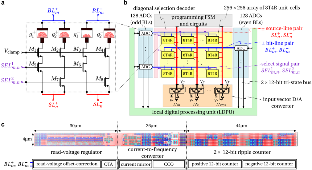
The image depicts a complex memory system architecture divided into three sections:
- **a**: Memory cell array with bit lines (BL), select lines (SL), and access transistors.
- **b**: System-level block diagram showing analog-to-digital conversion (ADC), programming logic, and digital processing.
- **c**: Signal processing chain including voltage regulation, current-to-frequency conversion, and digital counting.
### Components/Axes
#### Part a (Memory Cell Array)
- **Labels**:
- `BL_m+`/`BL_m-`: Bit lines (positive/negative).
- `SL_n+`/`SL_n-`: Select lines (positive/negative).
- `M1–M8`: Memory cells (likely 8T4R unit-cells).
- `g1–g2`: Access transistors.
- `Vclamp`: Clamp voltage source.
- `SEL1_m,n`/`SEL2_m,n`: Select signal pairs for row/column addressing.
- **Spatial Layout**:
- Bit lines (`BL_m+`, `BL_m-`) at the top.
- Memory cells (`M1–M8`) in the middle.
- Select lines (`SL_n+`, `SL_n-`) at the bottom.
#### Part b (System-Level Architecture)
- **Labels**:
- `8T4R unit-cells`: Memory cells with 8 transistors and 4 resistors.
- `128 ADCs`: Analog-to-digital converters for odd/even bit lines.
- `Programming FSM`: Finite state machine for write operations.
- `LDPU`: Local digital processing unit with ripple counters.
- `Input vector D/A converter`: Converts digital inputs to analog signals.
- **Flow**:
- Data flows from ADCs → Programming FSM → LDPU.
- Select signal pairs (`SEL1_m,n`, `SEL2_m,n`) control row/column access.
#### Part c (Signal Processing Chain)
- **Labels**:
- `Read-voltage regulator`: Stabilizes read voltage.
- `Current-to-frequency converter`: Converts current to frequency (CCO).
- `2x12-bit ripple counter`: Digitizes frequency into positive/negative counts.
- **Dimensions**:
- Read-voltage regulator: 30µm.
- Current-to-frequency converter: 26µm.
- Ripple counter: 44µm.
### Detailed Analysis
- **Part a**:
- The memory array uses cross-coupled transistors (`M1–M8`) to store data.
- Bit lines (`BL_m+`, `BL_m-`) and select lines (`SL_n+`, `SL_n-`) enable row/column addressing.
- `Vclamp` ensures stable voltage during read/write operations.
- **Part b**:
- The 256x256 array of 8T4R cells suggests high-density non-volatile memory (e.g., MRAM).
- Odd/even bit lines are processed by separate ADCs (128 ADCs total).
- The LDPU includes a 2x12-bit ripple counter for digital signal processing.
- **Part c**:
- The read-voltage regulator ensures consistent voltage for accurate ADC conversion.
- The current-to-frequency converter (CCO) digitizes analog current signals.
- Ripple counters handle overflow/underflow for 12-bit resolution.
### Key Observations
1. **Hybrid Analog-Digital Design**: Combines analog memory access (BL/SL) with digital processing (LDPU).
2. **High-Density Storage**: 256x256 array of 8T4R cells implies ~65,536 memory cells.
3. **Signal Integrity**: Clamp voltage and offset correction (OTA) mitigate noise in read operations.
4. **Scalability**: Modular components (e.g., 128 ADCs) allow expansion for larger memory arrays.
### Interpretation
This architecture represents a **high-density, low-power memory system** optimized for analog-digital hybrid processing. The use of 8T4R cells suggests non-volatile storage (e.g., MRAM), while the LDPU enables on-chip computation, reducing data transfer latency. The current-to-frequency conversion and ripple counters indicate a focus on energy-efficient digital signal processing, critical for applications like AI accelerators or edge computing. The modular design (e.g., separate ADCs for odd/even BLs) highlights scalability and fault tolerance.