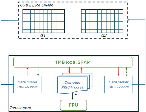
## Diagram: Tensix Core Architecture
### Overview
The image is a block diagram illustrating the architecture of a Tensix core, including its memory hierarchy and processing units. It shows the interaction between 8GB DDR4 DRAM, local SRAM, RISC-V cores, and a Floating Point Unit (FPU).
### Components/Axes
* **8GB DDR4 DRAM:** Two blocks labeled "d1" and "d2" represent external memory. Each block is visually depicted as a grid.
* **1MB local SRAM:** A rectangular block representing on-chip memory.
* **Data mover RISC-V core:** Two blocks representing data movement units.
* **Compute RISC-V cores:** A stack of blocks representing the main processing units.
* **FPU:** A block representing the Floating Point Unit.
* **Tensix core:** A large rectangular block encompassing the SRAM, Data movers, Compute cores, and FPU.
* **Arrows:** Indicate the direction of data flow between components. Blue arrows indicate data flow between the DRAM and the Tensix core. Red arrows indicate data flow between the SRAM and the Data mover/Compute cores. Green dashed arrows indicate data flow between the SRAM and the Data mover cores. Black arrows indicate data flow between the Compute cores and the FPU.
### Detailed Analysis or ### Content Details
* **8GB DDR4 DRAM:**
* Two identical blocks, each labeled "d1" and "d2" respectively, are positioned at the top of the diagram.
* Each block is labeled "8GB DDR4 DRAM".
* Each block contains a grid of 8 rows and 10 columns.
* **1MB local SRAM:**
* Located centrally within the "Tensix core" block.
* Labeled "1MB local SRAM".
* **Data mover RISC-V core:**
* Two blocks, one on the left and one on the right within the "Tensix core" block.
* Each labeled "Data mover RISC-V core".
* **Compute RISC-V cores:**
* A stack of three blocks in the center of the "Tensix core" block.
* Labeled "Compute RISC-V cores".
* **FPU:**
* A single block at the bottom of the "Tensix core" block.
* Labeled "FPU".
* **Tensix core:**
* The largest block, encompassing the SRAM, Data movers, Compute cores, and FPU.
* Labeled "Tensix core" at the bottom-left.
* **Data Flow:**
* Blue arrows connect the "8GB DDR4 DRAM" blocks to the "Data mover RISC-V core" blocks, indicating data transfer between external memory and the core.
* Red arrows connect the "1MB local SRAM" to the "Data mover RISC-V core" and "Compute RISC-V cores", indicating data transfer between the local SRAM and the processing units.
* Green dashed arrows connect the "1MB local SRAM" to the "Data mover RISC-V core", indicating data transfer between the local SRAM and the data movers.
* Black arrows connect the "Compute RISC-V cores" to the "FPU", indicating data transfer between the compute cores and the floating-point unit.
### Key Observations
* The diagram highlights a hierarchical memory structure: external DRAM and local SRAM.
* Data movers facilitate data transfer between external memory and the core.
* Compute cores perform the main processing tasks, potentially utilizing the FPU for floating-point operations.
### Interpretation
The diagram illustrates a typical architecture for a processing core designed for data-intensive tasks. The 8GB DDR4 DRAM provides large external memory, while the 1MB local SRAM offers faster access for frequently used data. The Data mover RISC-V cores handle data transfer between the external memory and the core's processing units. The Compute RISC-V cores perform the main computations, and the FPU accelerates floating-point operations. The architecture suggests a design optimized for parallel processing and efficient data movement.