\n
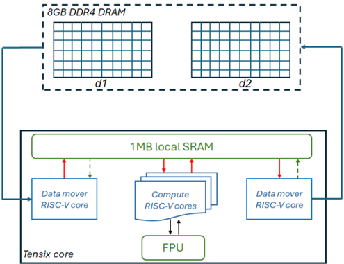
## Diagram: System Architecture - Memory and Processing Units
### Overview
The image depicts a system architecture diagram illustrating the relationship between external memory (DDR4 DRAM) and an integrated processing unit (Tensix core). The diagram highlights data flow between the memory and the core's components, including data movers, compute cores, and a floating-point unit (FPU).
### Components/Axes
The diagram consists of two main blocks:
* **Top Block:** Represents 8GB DDR4 DRAM, divided into two data sections labeled "d1" and "d2". This block is enclosed in a dashed blue rectangle.
* **Bottom Block:** Represents the "Tensix core", enclosed in a solid green rectangle. This block contains:
* "1MB local SRAM" – positioned at the top-center.
* Two "Data mover RISC-V core" blocks – positioned on the left and right sides.
* Multiple "Compute RISC-V cores" – positioned in the center.
* "FPU" – positioned at the bottom-center.
Arrows indicate data flow direction.
### Detailed Analysis or Content Details
* **DDR4 DRAM:** The diagram indicates 8GB of DDR4 DRAM, conceptually divided into two sections, d1 and d2. These sections appear as grid patterns, suggesting they represent memory arrays.
* **Data Flow:** Arrows show data moving from d1 and d2 in the DDR4 DRAM to the "Data mover RISC-V core" blocks within the Tensix core.
* **Data Mover RISC-V Cores:** These cores receive data from the DDR4 DRAM and transfer it to the "1MB local SRAM".
* **Local SRAM:** The 1MB local SRAM serves as an intermediate storage location.
* **Compute RISC-V Cores:** Data is transferred from the local SRAM to the "Compute RISC-V cores".
* **FPU:** The "Compute RISC-V cores" interact with the "FPU" (Floating Point Unit).
* **Interconnections:** The diagram shows bidirectional data flow between the local SRAM and the compute cores, and between the compute cores and the FPU.
### Key Observations
* The architecture emphasizes a hierarchical memory system with external DDR4 DRAM and internal SRAM.
* Dedicated "Data mover" cores are used to manage data transfer between external and internal memory.
* The FPU is tightly coupled with the compute cores, suggesting a focus on floating-point intensive computations.
* The diagram does not provide specific data transfer rates or bandwidths.
* The diagram does not provide information on the number of "Compute RISC-V cores".
### Interpretation
The diagram illustrates a heterogeneous computing architecture designed for efficient data processing. The separation of data movement and computation tasks into dedicated cores (Data movers and Compute cores) suggests an attempt to optimize performance and reduce bottlenecks. The use of local SRAM provides fast access to frequently used data, reducing the need to constantly access the slower DDR4 DRAM. The inclusion of an FPU indicates the system is well-suited for applications requiring high-precision floating-point calculations, such as machine learning or scientific simulations. The two data sections (d1 and d2) in the DDR4 DRAM could represent parallel data streams or separate memory banks for increased bandwidth. The diagram is a high-level overview and lacks quantitative details, but it provides a clear understanding of the system's key components and data flow.