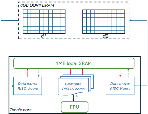
## Block Diagram: Tensix Core Computing Architecture
### Overview
The image is a technical block diagram illustrating the memory hierarchy and core components of a specialized computing architecture, likely an AI/ML accelerator or a high-performance processing unit. It depicts the data flow between an off-chip DRAM memory and an on-chip "Tensix core" containing local memory, specialized processing cores, and a floating-point unit.
### Components/Axes
The diagram is divided into two primary regions:
1. **Top Region (Off-Chip Memory):**
* **Label:** `8GB DDR4 DRAM`
* **Structure:** Represented by a dashed rectangular box containing two identical grid-like structures.
* **Sub-labels:** The left grid is labeled `d1`, and the right grid is labeled `d2`. These likely represent two distinct memory banks or channels within the DRAM.
2. **Bottom Region (On-Chip Tensix Core):**
* **Main Container:** A solid rectangular box labeled `Tensix core` in the bottom-left corner.
* **Central Memory:** A large, green-outlined rectangle at the top of the core labeled `1MB local SRAM`.
* **Processing Elements:**
* **Left:** A blue-outlined rectangle labeled `Data mover RISC-V core`.
* **Center:** A stack of three overlapping blue-outlined rectangles, with the top one labeled `Compute RISC-V cores`. This indicates multiple identical compute cores.
* **Right:** Another blue-outlined rectangle labeled `Data mover RISC-V core`.
* **Arithmetic Unit:** A green-outlined rectangle at the bottom-center labeled `FPU` (Floating Point Unit).
### Detailed Analysis
**Spatial Layout and Data Flow:**
* The `8GB DDR4 DRAM` is positioned at the top of the diagram, signifying it is external to the main processing core.
* The `Tensix core` occupies the lower, larger portion of the diagram.
* **Data Paths (Arrows):**
* A solid blue arrow originates from the left side of the `8GB DDR4 DRAM` box and points to the left `Data mover RISC-V core`.
* A solid blue arrow originates from the right side of the `8GB DDR4 DRAM` box and points to the right `Data mover RISC-V core`.
* **Within the Tensix Core:**
* **Red Arrows (Likely Write/Request):** Solid red arrows point from each `Data mover RISC-V core` and from the `Compute RISC-V cores` stack *upward* to the `1MB local SRAM`.
* **Green Dashed Arrows (Likely Read/Response):** Dashed green arrows point from the `1MB local SRAM` *downward* to each `Data mover RISC-V core`.
* **Compute-FPU Interaction:** Solid black arrows point bidirectionally (up and down) between the `Compute RISC-V cores` and the `FPU`, indicating a tight coupling for floating-point operations.
### Key Observations
1. **Hierarchical Memory:** The design features a clear two-level memory hierarchy: large, off-chip `8GB DDR4 DRAM` for capacity, and small, fast on-chip `1MB local SRAM` for low-latency access by the cores.
2. **Symmetrical Data Movement:** The architecture employs two dedicated `Data mover RISC-V cores`, each with a direct path to a separate bank (`d1`, `d2`) of the external DRAM. This suggests a design optimized for high memory bandwidth, potentially enabling concurrent read/write operations.
3. **Specialized Core Roles:** There is a clear separation of concerns:
* **Data Movers:** Handle data transfer between off-chip DRAM and on-chip SRAM.
* **Compute Cores:** Perform the primary computational tasks, accessing data from the local SRAM.
* **FPU:** A shared, specialized unit for floating-point arithmetic, used by the compute cores.
4. **Centralized Local Memory:** The `1MB local SRAM` acts as a shared scratchpad memory for all on-chip cores (both data movers and compute cores), facilitating efficient data sharing and reuse.
### Interpretation
This diagram outlines a **high-throughput, data-centric computing architecture**. The design prioritizes efficient data movement and parallel processing, which are critical for workloads like machine learning inference, scientific computing, or signal processing.
* **The dual data movers and split DRAM banks (`d1`, `d2`)** are a key architectural feature. They likely implement a double-buffering or ping-pong buffering scheme, allowing the compute cores to process one block of data from SRAM while the next block is being fetched from DRAM, thereby hiding memory latency and maximizing compute utilization.
* The use of **RISC-V cores** for both data movement and computation indicates a flexible, customizable design based on an open-source instruction set architecture.
* The **centralized FPU** suggests that floating-point operations are a common and performance-critical operation for the target workloads, warranting a dedicated, shared resource.
* The overall flow implies a pipeline: Data is moved from DRAM to SRAM by the data movers, processed by the compute cores (with help from the FPU), and the results are likely written back to DRAM via the data movers. The architecture is built to keep this pipeline full and minimize stalls due to memory access.