\n
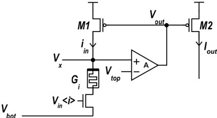
## Diagram: Operational Amplifier Circuit
### Overview
The image depicts a schematic diagram of an operational amplifier (op-amp) circuit, likely a current mirror configuration with feedback. The circuit consists of two MOSFETs (M1 and M2), an op-amp (labeled 'A'), and a third MOSFET (labeled with 'Gᵢ'). The diagram illustrates the connections and flow of signals within the circuit.
### Components/Axes
The diagram contains the following labeled components:
* **M1:** MOSFET, positioned at the top-left.
* **M2:** MOSFET, positioned at the top-right.
* **A:** Operational Amplifier, positioned in the center-right. The '+' and '-' signs indicate the non-inverting and inverting inputs, respectively.
* **Gᵢ:** MOSFET, positioned in the center-bottom.
* **V<sub>out</sub>:** Output voltage, positioned at the top-center.
* **V<sub>in</sub>:** Input voltage, positioned at the bottom-center.
* **V<sub>top</sub>:** Voltage at the top node, positioned to the right of Gᵢ.
* **V<sub>bot</sub>:** Voltage at the bottom node, positioned below Gᵢ.
* **i<sub>in</sub>:** Input current, positioned to the left of Gᵢ.
* **I<sub>out</sub>:** Output current, positioned below M2.
There are no axes in this diagram. It is a schematic representation, not a graph.
### Detailed Analysis / Content Details
The circuit operates as follows:
1. **Input:** The input voltage (V<sub>in</sub>) is applied to the gate of MOSFET Gᵢ.
2. **Current Flow:** The input current (i<sub>in</sub>) flows through MOSFET Gᵢ.
3. **Op-Amp Feedback:** The output voltage (V<sub>out</sub>) of the op-amp is connected to the gate of MOSFET M1. The op-amp attempts to maintain the voltage at the inverting input equal to the voltage at the non-inverting input.
4. **Current Mirroring:** MOSFETs M1 and M2 form a current mirror. The current flowing through M1 is mirrored by M2, resulting in an output current (I<sub>out</sub>).
5. **Voltage Regulation:** The op-amp provides feedback to regulate the output voltage (V<sub>out</sub>) and ensure that the current through M2 is proportional to the input current (i<sub>in</sub>).
The diagram does not provide specific numerical values for component parameters (e.g., resistance, capacitance, transistor characteristics). It is a conceptual representation of the circuit.
### Key Observations
* The circuit is designed to create a current mirror with feedback control.
* The op-amp is used to improve the accuracy and stability of the current mirror.
* The MOSFET Gᵢ acts as a current source controlled by the input voltage V<sub>in</sub>.
* The circuit is likely intended to provide a stable and predictable output current (I<sub>out</sub>) based on the input voltage (V<sub>in</sub>).
### Interpretation
This circuit is a classic example of a current mirror with an op-amp used for feedback and improved performance. The op-amp forces the voltage at the drain of M1 to be equal to V<sub>in</sub>, which in turn controls the current through M2. This configuration is commonly used in analog integrated circuit design for applications such as bias current generation, current sources, and active loads. The absence of specific component values suggests that the diagram is intended to illustrate the fundamental principle of operation rather than a specific implementation. The circuit's effectiveness relies on the matching characteristics of the MOSFETs and the performance of the op-amp. The feedback loop created by the op-amp ensures that the output current is relatively insensitive to variations in the op-amp's gain or the MOSFETs' threshold voltages.