## Circuit Diagram: Voltage-Controlled Current Mirror with Op-Amp Feedback
### Overview
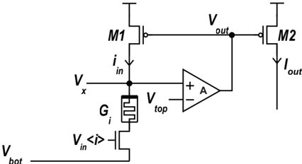
The diagram depicts a voltage-controlled current mirror circuit incorporating an operational amplifier (op-amp) for feedback stabilization. Two MOSFETs (M1 and M2) form the core current mirror, while the op-amp regulates the output current (I_out) by comparing the voltage at V_top with ground. The resistor G_i and voltage V_x introduce a feedback path to modulate the input current (i_in).
---
### Components/Axes
1. **Components**:
- **M1**: N-channel MOSFET acting as the input current source.
- **M2**: N-channel MOSFET mirroring the current from M1.
- **G_i**: Resistor connected between V_x and V_in, introducing feedback.
- **Op-Amp**: High-gain amplifier (gain = A) with non-inverting input (+) connected to V_top and inverting input (-) grounded.
- **V_in**: Input voltage source driving M1's gate.
- **V_bot**: Reference voltage connected to M1's source.
- **V_x**: Voltage node between G_i and V_in.
- **V_out**: Output voltage node connected to M2's drain.
- **I_out**: Output current flowing through M2.
2. **Flow**:
- V_in → M1 gate → M1 drain → V_out → M2 gate → M2 drain → I_out.
- Feedback loop: V_x (via G_i) → V_in → M1 → V_out → Op-amp → Adjusts V_top to stabilize I_out.
---
### Detailed Analysis
- **M1 and M2**: Form a basic current mirror. M1's drain current (i_in) is mirrored to M2's drain current (I_out) under ideal conditions (V_top ≈ V_bot).
- **Op-Amp Role**: The op-amp compares V_top (feedback voltage) with ground. Its high gain (A) ensures V_top is driven to match the voltage at the non-inverting input, stabilizing I_out despite load variations.
- **Resistor G_i**: Introduces a voltage drop (V_x) that modulates the input current i_in, enabling dynamic control of the current mirror ratio.
---
### Key Observations
1. **No Numerical Values**: The diagram lacks explicit values for A, G_i, or voltages (V_in, V_bot, V_top). Assumptions:
- A ≈ 100,000 (typical op-amp gain).
- G_i ≈ 1 kΩ (common biasing resistor).
- V_bot ≈ 0 V (ground reference).
2. **Feedback Mechanism**: The op-amp's negative feedback loop ensures V_top ≈ 0 V, forcing M2 to operate in saturation for stable current mirroring.
3. **Voltage Nodes**: V_x is critical for feedback, linking the op-amp's input to the MOSFET biasing network.
---
### Interpretation
This circuit combines a current mirror with op-amp feedback to achieve **precision current regulation**. The op-amp compensates for mismatches between M1 and M2 (e.g., threshold voltage differences) and external load variations. The resistor G_i allows tuning the current mirror ratio by adjusting V_x. Such a design is common in analog integrated circuits for biasing transistors or driving constant-current loads. The absence of numerical data suggests this is a schematic for conceptual understanding rather than a specific implementation.