## Circuit Diagram: LBM-Based Neuron Circuit
### Overview
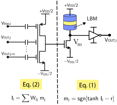
The image presents a circuit diagram of an LBM (likely a Logic-Based Memory or similar) based neuron circuit. The diagram is split into two sections, separated by a dashed vertical line. The left side shows a summation circuit, and the right side shows the LBM and an inverter. The diagram includes voltage labels, component symbols, and mathematical equations.
### Components/Axes
* **Left Side:**
* Input voltages: Vbias,i, VOUT,j, VOUT,j+n (with an ellipsis indicating potentially more inputs).
* Capacitors connected to each input voltage.
* A transistor connected to the capacitors.
* Voltage source: +VDD/2 at the top of the transistor.
* Voltage source: -VDD/2 at the bottom of the transistor.
* **Right Side:**
* LBM (Logic-Based Memory) represented as a cylinder with two distinct layers (likely representing different magnetic states).
* Voltage source: +VDD/2 connected to the top of the LBM.
* Transistor connected to the LBM.
* Voltage source: -VDD/2 at the bottom of the transistor.
* Voltage label: Vm at the connection between the LBM and the transistor.
* Inverter connected to the transistor.
* Output voltage: VOUT,i.
* **Equations:**
* Eq. (2): Ii = Σ Wij mj (located on the left side)
* Eq. (1): mi = sgn[tanh Ii - r] (located on the right side)
### Detailed Analysis or Content Details
* **Left Side (Summation Circuit):**
* Multiple input voltages (Vbias,i, VOUT,j, VOUT,j+n) are connected to capacitors.
* These capacitors are connected to the gate of a transistor.
* The transistor is biased with +VDD/2 at the top and -VDD/2 at the bottom.
* The equation Ii = Σ Wij mj suggests that the transistor is performing a weighted sum of the inputs.
* **Right Side (LBM and Inverter):**
* The LBM is connected to a transistor, which is biased with +VDD/2 and -VDD/2.
* The voltage at the connection between the LBM and the transistor is labeled Vm.
* An inverter is connected to the transistor, producing the output voltage VOUT,i.
* The equation mi = sgn[tanh Ii - r] suggests that the LBM's state (mi) is determined by a hyperbolic tangent function of the input current (Ii) minus a threshold (r), and then passed through a signum function.
* **Voltage Levels:**
* +VDD/2 and -VDD/2 are used as voltage sources in the circuit.
* Vbias,i, VOUT,j, VOUT,j+n, Vm, and VOUT,i are voltage labels at different points in the circuit.
### Key Observations
* The circuit appears to implement a neuron-like function, where the left side performs a weighted sum of inputs, and the right side uses an LBM and an inverter to produce an output.
* The equations provide a mathematical description of the circuit's behavior.
* The LBM is a key component of the circuit, likely providing a non-linear activation function.
### Interpretation
The circuit diagram illustrates a potential implementation of a neuron using an LBM. The left side of the circuit performs a weighted summation of input voltages, which is a common operation in neural networks. The right side of the circuit uses the LBM to introduce a non-linearity, which is also essential for neural network functionality. The equation mi = sgn[tanh Ii - r] suggests that the LBM's state is determined by a hyperbolic tangent function, which is a common activation function in neural networks. The inverter likely serves to invert the signal from the LBM, providing the final output of the neuron. This circuit could be used as a building block for larger neural networks.