## Circuit Diagram: Memristor-Based Neuron Circuit with Weighted Summation and Activation
### Overview
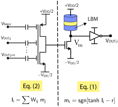
The image is a technical circuit schematic diagram illustrating a two-stage electronic neuron circuit, likely for neuromorphic computing. It is divided into two distinct sections by a vertical dashed line. The left section implements a weighted summation of inputs, and the right section performs a nonlinear activation function using a memristor device. Mathematical equations corresponding to each stage are provided below their respective circuit sections.
### Components/Axes
**Left Section (Weighted Summation Stage):**
* **Inputs:** Three labeled input terminals on the far left: `Vbias,i`, `Vout,j`, and `Vout,j+n` (with ellipsis `...` indicating multiple similar inputs).
* **Components:** Each input is connected through a capacitor (symbolized by two parallel lines) to the gate of a p-channel MOSFET transistor.
* **Power Rails:** The transistor's source is connected to `+VDD/2` and its drain to `-VDD/2`.
* **Output:** The drain of the transistor connects to the central vertical dashed line, serving as the output of this stage.
**Right Section (Activation Stage):**
* **Input:** The signal from the left stage connects to the gate of an n-channel MOSFET transistor.
* **Memristor:** A device labeled `LBM` (likely "Linear Boundary Memristor" or similar) is connected between the `+VDD/2` rail and the drain of the n-channel transistor. It is depicted as a cylindrical component with blue and yellow bands.
* **Transistor:** The n-channel MOSFET's source is connected to `-VDD/2`.
* **Intermediate Node:** The connection point between the memristor and the transistor drain is labeled `Vm`.
* **Output Stage:** The node `Vm` feeds into a logic inverter (triangle with a circle at the output). The output of this inverter is the final circuit output, labeled `VOUT,i`.
**Equations:**
* **Below Left Section:** A yellow-highlighted box contains `Eq. (2)`: `Ii = Σ wij mj`
* **Below Right Section:** A yellow-highlighted box contains `Eq. (1)`: `mi = sgn[tanh Ii - r]`
### Detailed Analysis
**Circuit Flow and Connections:**
1. **Signal Path:** The diagram shows a clear left-to-right signal flow. Multiple input voltages (`Vbias,i`, `Vout,j`, etc.) are capacitively coupled to modulate the conductance of the p-FET. The resulting current or voltage at the p-FET's drain represents a weighted sum.
2. **Stage Separation:** The vertical dashed line clearly demarcates the summation circuit (left) from the activation circuit (right).
3. **Memristor Role:** The `LBM` memristor acts as a programmable or stateful element in the right stage. Its resistance likely defines a threshold or weight for the activation function.
4. **Final Output:** The inverter at the end suggests the final output `VOUT,i` is a digital or strongly nonlinear signal derived from the analog voltage `Vm`.
**Equation Transcription:**
* **Eq. (2):** `Ii = Σ wij mj`
* `Ii`: Likely the total input current or integrated signal for neuron `i`.
* `Σ`: Summation symbol.
* `wij`: Weight connecting presynaptic neuron `j` to neuron `i`.
* `mj`: State or output of presynaptic neuron `j`.
* **Eq. (1):** `mi = sgn[tanh Ii - r]`
* `mi`: Output state of neuron `i`.
* `sgn`: Sign function (outputs +1 or -1, or 1/0).
* `tanh`: Hyperbolic tangent function, a common sigmoidal activation.
* `Ii`: Input from Eq. (2).
* `r`: A bias or threshold parameter.
### Key Observations
1. **Hybrid Analog/Digital Design:** The circuit combines analog processing (capacitive coupling, memristor, tanh function implied by circuit behavior) with digital-like output (sgn function, inverter).
2. **Use of Mid-Rail Voltages:** Both `+VDD/2` and `-VDD/2` are used as power supplies, indicating a bipolar signaling scheme centered around 0V.
3. **Memristor as Key Element:** The `LBM` memristor is the central, distinctive component in the activation stage, suggesting this circuit is designed for in-memory computing or synaptic plasticity.
4. **Clear Mathematical Mapping:** The physical circuit components directly map to the mathematical operations in the equations: the left circuit performs the weighted sum (`Σ wij mj`), and the right circuit, with the memristor and transistor, implements the nonlinear activation (`sgn[tanh Ii - r]`).
### Interpretation
This diagram represents the hardware implementation of an artificial neuron's core computation: **weighted summation followed by a nonlinear activation**.
* **What it demonstrates:** It shows how standard CMOS transistors can be combined with a memristor to create a compact, potentially low-power neuron circuit suitable for neuromorphic hardware. The capacitive inputs suggest a method for signal integration or charge-based computation.
* **Relationship between elements:** The left stage is the "dendritic" input collector, performing integration. The right stage is the "somatic" activation unit, where the memristor's state (`r` in the equation) likely sets the neuron's firing threshold. The inverter ensures a clean output pulse.
* **Notable implications:** The use of `tanh` and `sgn` in the equation points to a bipolar neuron model (outputs -1/+1). The circuit likely operates in the subthreshold or weak inversion region to approximate these functions with analog components. The `LBM` memristor's state could be programmable, allowing the neuron's threshold (`r`) to be tuned, which is fundamental for learning in neural networks.
**Language Declaration:** All text in the image is in English, using standard technical and mathematical notation.