## Device Schematics and Electrical Characteristics
### Overview
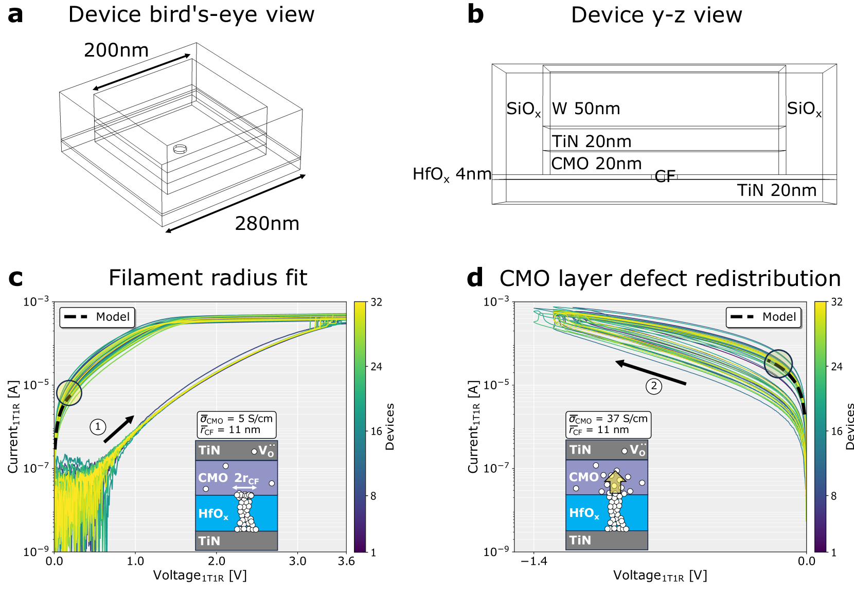
The image presents device schematics and electrical characteristics related to a resistive switching memory device. It includes two device views (bird's-eye and y-z) and two plots showing the current-voltage (I-V) characteristics for multiple devices under different conditions.
### Components/Axes
**Panel a: Device bird's-eye view**
* Title: Device bird's-eye view
* Dimensions: 200 nm x 280 nm (approximate)
**Panel b: Device y-z view**
* Title: Device y-z view
* Layers (from top to bottom):
* SiO<sub>x</sub>, W 50nm, SiO<sub>x</sub>
* TiN 20nm
* CMO 20nm
* CF (Conductive Filament)
* TiN 20nm
* HfO<sub>x</sub> 4nm
**Panel c: Filament radius fit**
* Title: Filament radius fit
* X-axis: Voltage<sub>1T1R</sub> [V]
* Scale: Linear, from 0.0 to 3.6
* Y-axis: Current<sub>1T1R</sub> [A]
* Scale: Logarithmic, from 10<sup>-9</sup> to 10<sup>-3</sup>
* Right Y-axis: Devices
* Scale: Linear, from 1 to 32
* Legend:
* Model (black dashed line)
* Inset Diagram:
* Layers (from top to bottom): TiN, CMO, HfO<sub>x</sub>, TiN
* Annotations: V<sub>O</sub><sup>••</sup>, 2r<sub>CF</sub>
* Parameters: σ<sub>CMO</sub> = 5 S/cm, r<sub>CF</sub> = 11 nm
* Arrow 1: Indicates the general trend of the I-V curves.
**Panel d: CMO layer defect redistribution**
* Title: CMO layer defect redistribution
* X-axis: Voltage<sub>1T1R</sub> [V]
* Scale: Linear, from -1.4 to 0.0
* Y-axis: Current<sub>1T1R</sub> [A]
* Scale: Logarithmic, from 10<sup>-9</sup> to 10<sup>-3</sup>
* Right Y-axis: Devices
* Scale: Linear, from 1 to 32
* Legend:
* Model (black dashed line)
* Inset Diagram:
* Layers (from top to bottom): TiN, CMO, HfO<sub>x</sub>, TiN
* Annotations: V<sub>O</sub><sup>••</sup>
* Parameters: σ<sub>CMO</sub> = 37 S/cm, r<sub>CF</sub> = 11 nm
* Arrow 2: Indicates the general trend of the I-V curves.
### Content Details
**Panel c: Filament radius fit**
* The plot shows multiple I-V curves, each representing a different device. The color of each curve corresponds to the number of devices, ranging from dark blue (1 device) to yellow (32 devices).
* The I-V curves generally show an increase in current with increasing voltage.
* At low voltages (near 0V), the current is very low (around 10<sup>-9</sup> A).
* As the voltage increases, the current increases sharply, reaching values around 10<sup>-3</sup> A at higher voltages (around 3.6V).
* The "Model" curve (black dashed line) represents a theoretical fit to the experimental data. It closely follows the average trend of the I-V curves.
* The inset diagram illustrates the device structure with the conductive filament (CF) formation in the HfO<sub>x</sub> layer. The CMO layer is also shown with oxygen vacancies (V<sub>O</sub><sup>••</sup>).
* The conductivity of the CMO layer (σ<sub>CMO</sub>) is given as 5 S/cm, and the radius of the conductive filament (r<sub>CF</sub>) is 11 nm.
**Panel d: CMO layer defect redistribution**
* Similar to panel c, this plot shows multiple I-V curves for different devices, colored according to the number of devices.
* The voltage range is from -1.4V to 0.0V.
* The I-V curves show a general decrease in current as the voltage becomes more negative.
* The current values range from around 10<sup>-3</sup> A at 0V to lower values (around 10<sup>-9</sup> A) at -1.4V.
* The "Model" curve (black dashed line) represents a theoretical fit to the experimental data.
* The inset diagram illustrates the device structure with the CMO layer defect redistribution. The CMO layer is shown with oxygen vacancies (V<sub>O</sub><sup>••</sup>).
* The conductivity of the CMO layer (σ<sub>CMO</sub>) is given as 37 S/cm, and the radius of the conductive filament (r<sub>CF</sub>) is 11 nm.
### Key Observations
* The device schematics in panels a and b provide a visual representation of the device structure and dimensions.
* The I-V curves in panels c and d show the electrical characteristics of the device under different conditions.
* The conductivity of the CMO layer (σ<sub>CMO</sub>) is different in panels c and d (5 S/cm vs. 37 S/cm), indicating a change in the material properties.
* The radius of the conductive filament (r<sub>CF</sub>) is the same in both panels (11 nm).
* The "Model" curves provide a theoretical fit to the experimental data, which can be used to understand the underlying physical mechanisms.
### Interpretation
The data suggests that the resistive switching behavior of the device is influenced by the CMO layer and the formation/redistribution of oxygen vacancies. The change in conductivity of the CMO layer between panels c and d indicates that the material properties are being modified, possibly due to the redistribution of defects. The conductive filament formation in the HfO<sub>x</sub> layer plays a crucial role in the switching mechanism. The I-V curves show the relationship between voltage and current, which is essential for understanding the device's performance. The "Model" curves provide a theoretical framework for interpreting the experimental data and understanding the underlying physical mechanisms. The difference in the CMO conductivity between the two plots suggests that the defect redistribution process significantly impacts the device's electrical characteristics.