## Scientific Diagram: Device Structure and Filament Characteristics
### Overview
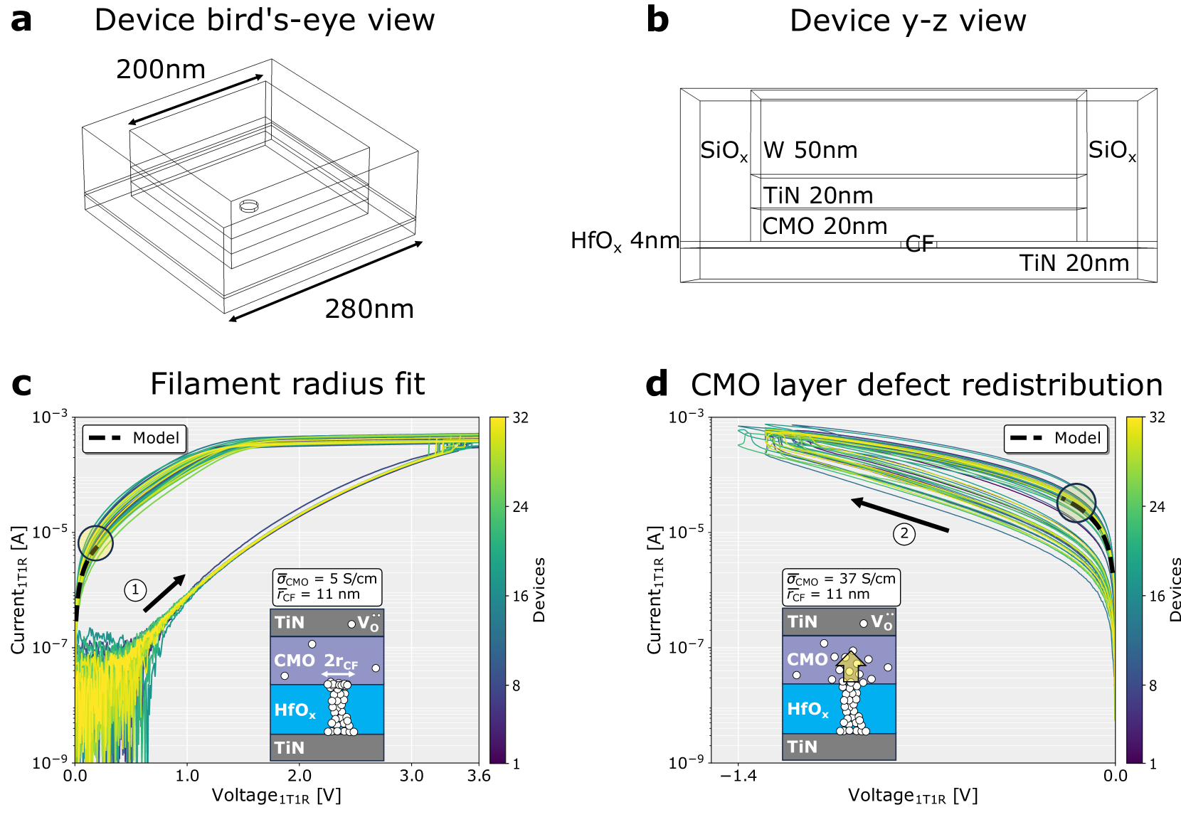
The image presents a series of diagrams illustrating the structure and electrical characteristics of a memristive device. It includes a bird's-eye view and a y-z cross-section of the device, followed by two graphs depicting filament radius fit and CMO layer defect redistribution under varying voltage conditions. The graphs utilize a color map to represent device count.
### Components/Axes
**a) Device bird's-eye view:**
- Dimensions: 200nm x 280nm
- Shows a rectangular device with circular electrodes.
**b) Device y-z view:**
- Layers: SiO<sub>x</sub> (50nm), TiN (20nm), CMO (20nm), HfO<sub>x</sub> (4nm), TiN (20nm).
- CF (presumably a conductive filament) is indicated.
**c) Filament radius fit:**
- X-axis: Voltage<sub>ITIR</sub> [V] (Scale: 0.0 to 3.6)
- Y-axis: Current<sub>ITIR</sub> [A] (Logarithmic scale: 10<sup>-9</sup> to 10<sup>-3</sup>)
- Color Map: Represents the number of devices (Scale: 1 to 32)
- Legend:
- Black dashed line: "Model"
- Circles: σ<sub>CMO</sub> = 5 S/cm, r<sub>CF</sub> = 11 nm
- Symbols: V<sub>o</sub>, CMO, 2r<sub>CF</sub>, TiN, HfO<sub>x</sub>
- Annotation: ①
**d) CMO layer defect redistribution:**
- X-axis: Voltage<sub>ITIR</sub> [V] (Scale: -1.4 to 0.0)
- Y-axis: Current<sub>ITIR</sub> [A] (Logarithmic scale: 10<sup>-7</sup> to 10<sup>-3</sup>)
- Color Map: Represents the number of devices (Scale: 1 to 32)
- Legend:
- Black dashed line: "Model"
- Circles: σ<sub>CMO</sub> = 37 S/cm, r<sub>CF</sub> = 11 nm
- Symbols: V<sub>o</sub>, CMO, 2r<sub>CF</sub>, TiN, HfO<sub>x</sub>
- Annotation: ②
### Detailed Analysis or Content Details
**a) Device bird's-eye view:**
- The device is a rectangular structure with dimensions approximately 200nm x 280nm.
- Two circular electrodes are visible.
**b) Device y-z view:**
- The device consists of several layers: SiO<sub>x</sub>, TiN, CMO, HfO<sub>x</sub>, and TiN.
- The thicknesses of each layer are indicated: SiO<sub>x</sub> (50nm), TiN (20nm), CMO (20nm), HfO<sub>x</sub> (4nm), TiN (20nm).
- A conductive filament (CF) is shown extending through the layers.
**c) Filament radius fit:**
- The graph shows multiple curves representing the current-voltage (I-V) characteristics of the device.
- The curves generally exhibit a sharp increase in current at a specific voltage, followed by saturation.
- The color map indicates that the highest device counts (darker green, around 32) are concentrated at lower voltages (around 0.5-1.5V) and moderate current levels (around 10<sup>-6</sup> to 10<sup>-5</sup> A).
- The "Model" (dashed black line) shows a similar trend to the experimental data.
- The circles represent a specific set of parameters: σ<sub>CMO</sub> = 5 S/cm and r<sub>CF</sub> = 11 nm.
- The annotation ① points to the initial rise in current.
**d) CMO layer defect redistribution:**
- Similar to (c), this graph displays I-V characteristics.
- The curves are shifted towards negative voltages compared to graph (c).
- The highest device counts (darker green, around 32) are concentrated at negative voltages (around -0.5 to -1.0V) and moderate current levels (around 10<sup>-6</sup> to 10<sup>-5</sup> A).
- The "Model" (dashed black line) shows a similar trend to the experimental data.
- The circles represent a different set of parameters: σ<sub>CMO</sub> = 37 S/cm and r<sub>CF</sub> = 11 nm.
- The annotation ② points to the initial rise in current.
### Key Observations
- The I-V curves in both graphs (c) and (d) demonstrate memristive behavior, characterized by a non-linear relationship between current and voltage.
- The color maps reveal that the device performance is sensitive to voltage and current levels.
- The two graphs show different voltage ranges and parameter sets, suggesting that the device characteristics can be tuned by adjusting material properties (σ<sub>CMO</sub>) and filament radius (r<sub>CF</sub>).
- The "Model" closely matches the experimental data in both graphs, indicating the model's validity.
- The shift in I-V curves between (c) and (d) suggests a change in the dominant switching mechanism or defect distribution within the CMO layer.
### Interpretation
The diagrams illustrate the structure and electrical behavior of a resistive switching memory device. The device consists of a stack of thin films, including SiO<sub>x</sub>, TiN, CMO, and HfO<sub>x</sub>, with a conductive filament (CF) forming the switching element.
The I-V characteristics shown in graphs (c) and (d) demonstrate the memristive effect, where the resistance of the device changes depending on the history of applied voltage. The color maps provide insights into the distribution of device performance, revealing that certain voltage and current ranges yield higher device counts.
The differences between graphs (c) and (d) suggest that the CMO layer plays a crucial role in the switching mechanism. The change in conductivity (σ<sub>CMO</sub>) and the filament radius (r<sub>CF</sub>) influence the I-V characteristics and device performance. The annotations ① and ② highlight the initial switching events, indicating the voltage thresholds for filament formation or rupture.
The close agreement between the experimental data and the "Model" suggests that the underlying physics of the device is well understood. This information can be used to optimize the device structure and material properties for improved performance and reliability. The defect redistribution in the CMO layer, as indicated in graph (d), is likely a key factor in the switching process and warrants further investigation.