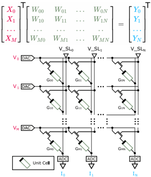
## Matrix Multiplication Circuit Diagram
### Overview
The image presents a circuit diagram illustrating a matrix multiplication operation. It shows an array of unit cells, each containing a memristor, arranged in a grid. The diagram also includes input voltages (V0 to VM), digital-to-analog converters (DACs), analog-to-digital converters (ADCs), and output currents (I0 to IN). The matrix multiplication is represented mathematically at the top of the diagram.
### Components/Axes
* **Mathematical Representation (Top):**
* **Left Matrix (X):** A column vector with elements X0, X1, ..., XM. The vector is transposed (T). The elements are colored red.
* **Middle Matrix (W):** A matrix with elements W00, W01, ..., W0N, W10, W11, ..., W1N, ..., WM0, WM1, ..., WMN.
* **Right Matrix (Y):** A column vector with elements Y0, Y1, ..., YN. The vector is transposed (T). The elements are colored blue.
* The equation represents X * W = Y.
* **Circuit Diagram (Center):**
* **Input Voltages:** V0, V1, ..., VM. Each connected to a DAC.
* **DACs:** Digital-to-Analog Converters, converting digital inputs to analog voltages.
* **Memristor Array:** A grid of memristors, each labeled G00, G01, ..., G0N, G10, G11, ..., G1N, ..., GM0, GM1, ..., GMN.
* **Output Currents:** I0, I1, ..., IN. Each connected to an ADC. The elements are colored blue.
* **ADCs:** Analog-to-Digital Converters, converting analog currents to digital outputs.
* **Vertical Lines:** Labeled V_SL0, V_SL1, ..., V_SLN.
* **Legend (Bottom-Left):**
* "Unit Cell" is represented by a rectangular block with a diagonal line.
### Detailed Analysis or Content Details
* **Matrix Multiplication:** The mathematical representation at the top shows the matrix multiplication being performed by the circuit. The input vector X is multiplied by the weight matrix W to produce the output vector Y.
* **Circuit Operation:** The input voltages V0 to VM are converted to analog signals by the DACs. These voltages are applied to the rows of the memristor array. The memristors act as variable resistors, and their conductances (G) represent the elements of the weight matrix W. The output currents I0 to IN are proportional to the product of the input voltages and the memristor conductances. These currents are converted to digital signals by the ADCs.
* **Unit Cell:** Each unit cell in the array contains a memristor. The conductance of the memristor can be programmed to represent a specific weight value.
* **Grid Structure:** The memristors are arranged in a grid, with each row corresponding to an input voltage and each column corresponding to an output current. The vertical lines are labeled V_SL0, V_SL1, ..., V_SLN.
### Key Observations
* The circuit diagram implements matrix multiplication using a memristor array.
* The memristor conductances represent the elements of the weight matrix.
* The input voltages represent the elements of the input vector.
* The output currents represent the elements of the output vector.
### Interpretation
The diagram illustrates a hardware implementation of matrix multiplication using memristors. This approach offers potential advantages in terms of speed, power consumption, and area compared to traditional digital implementations. The memristor array allows for parallel computation of the matrix multiplication, which can significantly speed up the process. The use of analog signals also reduces the power consumption compared to digital circuits. This type of architecture is relevant for applications such as machine learning, where matrix multiplication is a fundamental operation. The diagram shows how the mathematical operation is mapped onto a physical circuit, highlighting the relationship between the abstract mathematical concept and its concrete implementation.