## Diagram: Memristor Crossbar Array for Matrix-Vector Multiplication
### Overview
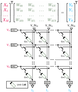
The image illustrates the mathematical and physical implementation of a matrix-vector multiplication operation using a crossbar array architecture. The top section displays the mathematical equation $[X]^T \times [W] = [Y]^T$, while the bottom section provides the corresponding circuit diagram, where memristors (labeled as "Unit Cell") act as programmable conductance elements ($G_{ij}$) to perform the computation in the analog domain.
### Components/Axes
**Mathematical Equation (Top Section):**
* **Input Vector ($X$):** Represented in red text as a column vector $[X_0, X_1, \dots, X_M]^T$.
* **Weight Matrix ($W$):** Represented in green text as an $M \times N$ matrix containing elements $W_{00}$ through $W_{MN}$.
* **Output Vector ($Y$):** Represented in blue text as a column vector $[Y_0, Y_1, \dots, Y_N]^T$.
**Circuit Diagram (Bottom Section):**
* **Row Inputs:** $V_0, V_1, \dots, V_M$. Each row is driven by a Digital-to-Analog Converter (DAC).
* **Column Outputs:** $I_0, I_1, \dots, I_N$. Each column is read by an Analog-to-Digital Converter (ADC).
* **Vertical Lines:** Labeled as $V\_SL_0, V\_SL_1, \dots, V\_SL_N$ (Source Lines).
* **Cross-point Elements:** Each intersection of a row and column contains a transistor and a "Unit Cell" (memristor) with conductance $G_{ij}$.
* **Legend (Bottom Left):** A box containing a rectangle with a filled top segment, labeled "Unit Cell".
### Detailed Analysis
**Mathematical Mapping:**
The equation $[X]^T \times [W] = [Y]^T$ is physically realized by the crossbar array:
* **Inputs ($X_i$):** The input vector elements are converted into voltages ($V_i$) applied to the rows of the crossbar.
* **Weights ($W_{ij}$):** The matrix elements are stored as physical conductance values ($G_{ij}$) within the memristors at each cross-point.
* **Outputs ($Y_j$):** The output vector elements are obtained as currents ($I_j$) flowing through the columns, which are then converted back to digital values via ADCs.
**Circuit Topology:**
* **Row Structure:** Each row $i$ (from $0$ to $M$) is connected to a DAC. The voltage $V_i$ is applied to the gate of a transistor, which controls the current flowing through the memristor $G_{ij}$ into the vertical column line.
* **Column Structure:** Each column $j$ (from $0$ to $N$) aggregates the currents from all rows. The total current $I_j$ in column $j$ is the summation of the currents from each row, effectively performing the dot product: $I_j = \sum_{i=0}^{M} V_i \times G_{ij}$.
* **Connectivity:** The diagram uses ellipses ($\dots$) to indicate that the array scales to $M$ rows and $N$ columns.
### Key Observations
* **Color Coding:** The image uses a consistent color scheme to link the math to the hardware:
* **Red:** Input vector $X$ corresponds to the row inputs ($V_0 \dots V_M$).
* **Green:** Weight matrix $W$ corresponds to the conductance values ($G_{00} \dots G_{MN}$).
* **Blue:** Output vector $Y$ corresponds to the column outputs ($I_0 \dots I_N$).
* **Unit Cell:** The "Unit Cell" symbol (a rectangle with a black top) is the fundamental building block of this architecture, representing a non-volatile memory element (likely a memristor or RRAM cell) capable of storing a weight value as conductance.
* **Scalability:** The use of ellipses in both the matrix and the circuit diagram indicates that this architecture is designed to be scalable to large dimensions ($M \times N$).
### Interpretation
This diagram depicts an **Analog In-Memory Computing (AIMC)** architecture.
* **Functionality:** By storing the weights of a neural network as conductance values ($G_{ij}$) in a crossbar array, the system can perform Matrix-Vector Multiplication (MVM) in a single clock cycle using Ohm's Law ($I=V \times G$) and Kirchhoff's Current Law (summation of currents).
* **Efficiency:** This approach bypasses the "von Neumann bottleneck," where data must be moved between memory and the processor. Here, the memory *is* the processor.
* **Application:** This is a standard design for hardware accelerators used in deep learning inference, allowing for massive parallelism and energy efficiency compared to traditional digital CMOS-based matrix multiplication. The DACs and ADCs are the necessary interfaces to bridge the analog computing core with the digital world.