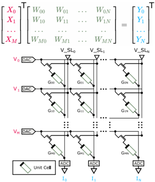
## Diagram: Analog Matrix Multiplier Circuit with Mathematical Representation
### Overview
The image is a technical diagram illustrating the hardware implementation of a matrix multiplication operation using an analog resistive crossbar array. It consists of two main parts: a mathematical matrix equation at the top and a corresponding circuit schematic below. The diagram demonstrates how input voltages (X) are multiplied by a matrix of conductances (W) to produce output currents (Y).
### Components/Axes
#### 1. Mathematical Representation (Top Section)
* **Equation Structure:** `X^T * W = Y^T`
* **Input Vector (X):** A column vector labeled `X` in **purple**. Elements are `X₀, X₁, ..., Xₘ`.
* **Weight Matrix (W):** A matrix labeled `W` in **black**. It has `(M+1)` rows and `(N+1)` columns.
* Row indices: `0` to `M`.
* Column indices: `0` to `N`.
* Elements: `W₀₀, W₀₁, ..., W₀ₙ` (first row) down to `Wₘ₀, Wₘ₁, ..., Wₘₙ` (last row).
* **Output Vector (Y):** A column vector labeled `Y` in **blue**. Elements are `Y₀, Y₁, ..., Yₙ`.
* **Spatial Layout:** The equation is centered at the top of the image. The `X` vector is on the left, the `W` matrix in the center, and the `Y` vector on the right.
#### 2. Circuit Schematic (Main Section)
* **Input Stage (Left Side):**
* A vertical column of voltage sources labeled `V₀, V₁, ..., Vₘ`.
* Each voltage source is connected to a block labeled **"DAC"** (Digital-to-Analog Converter).
* **Core Crossbar Array (Center):**
* A grid of interconnected lines forming a crossbar structure.
* Horizontal lines are driven by the input voltages (`V₀` to `Vₘ`) from the DACs.
* Vertical lines are connected to the output stage.
* At each crosspoint (intersection of a horizontal and vertical line), there is a **"Unit Cell"**.
* **Unit Cell Symbol:** A rectangle containing a resistor symbol and a switch symbol. The legend at the bottom-left confirms this symbol represents a "Unit Cell".
* **Conductance Labels:** Each unit cell is labeled with a conductance value `Gᵢⱼ`, where `i` is the row index (0 to M) and `j` is the column index (0 to N). Examples: `G₀₀, G₀₁, ..., G₀ₙ` (top row), `G₁₀, G₁₁, ..., G₁ₙ` (second row), down to `Gₘ₀, Gₘ₁, ..., Gₘₙ` (bottom row).
* **Control Signals:** Vertical control lines labeled `V_SL₀, V_SL₁, ..., V_SLₙ` are shown entering the top of the array, likely for programming the conductance values of the unit cells in each column.
* **Output Stage (Bottom):**
* The bottom of each vertical line in the crossbar array is connected to a block labeled **"ADC"** (Analog-to-Digital Converter).
* The outputs of these ADCs are labeled as currents `I₀, I₁, ..., Iₙ` in **blue**, corresponding to the mathematical output vector `Y`.
* **Spatial Layout:** The DACs are aligned vertically on the left. The crossbar array occupies the central area. The ADCs are aligned horizontally at the bottom. The unit cell legend is in the bottom-left corner.
### Detailed Analysis
* **Function Mapping:** The circuit is a direct physical implementation of the matrix equation.
* The input vector `X` (purple) corresponds to the analog input voltages `V₀...Vₘ` (after DAC conversion).
* The weight matrix `W` (black) is stored as the conductance values `G₀₀...Gₘₙ` in the crossbar array. The relationship is `Wᵢⱼ ∝ Gᵢⱼ`.
* The output vector `Y` (blue) corresponds to the measured output currents `I₀...Iₙ` (before ADC conversion). The fundamental circuit law (Ohm's Law and Kirchhoff's Current Law) dictates that `Iⱼ = Σᵢ (Vᵢ * Gᵢⱼ)`, which is the matrix multiplication `Yⱼ = Σᵢ (Xᵢ * Wᵢⱼ)`.
* **Signal Flow:** The flow is from left to right and top to bottom.
1. Digital inputs are converted to analog voltages (`V`) by the DACs.
2. These voltages are applied to the rows of the conductance crossbar.
3. The crossbar performs the analog multiply-accumulate (MAC) operation.
4. The resulting currents (`I`) on each column are digitized by the ADCs.
* **Scalability:** The use of ellipses (`...`) for indices (`0...M`, `0...N`) indicates the architecture is scalable to large matrix dimensions.
### Key Observations
1. **Color-Coded Correspondence:** There is a strict color link between the mathematical model and the circuit implementation:
* **Purple:** Input vector `X` ↔ Input voltages `V`.
* **Blue:** Output vector `Y` ↔ Output currents `I`.
* **Black:** Weight matrix `W` ↔ Conductance matrix `G`.
2. **Hybrid System:** The diagram explicitly shows the interface between digital and analog domains via DACs (input) and ADCs (output), framing the crossbar as an analog compute core within a larger digital system.
3. **Programmability:** The presence of `V_SL` (Source Line Voltage) control signals and switches within the unit cell symbol implies that the conductance values `Gᵢⱼ` are programmable, allowing the weight matrix `W` to be updated.
### Interpretation
This diagram represents a **neuromorphic or analog computing architecture** designed for efficient matrix-vector multiplication, a fundamental operation in signal processing, control systems, and especially artificial neural networks (e.g., the inference step in a dense layer).
* **What it demonstrates:** It shows how a complex mathematical operation (`Y = XW`) can be mapped directly onto the physical properties of a circuit (Ohm's Law for multiplication, Kirchhoff's Law for summation). This "compute-in-memory" approach avoids the von Neumann bottleneck of moving data between separate memory and processor units.
* **Why it matters:** Analog crossbar arrays promise orders-of-magnitude improvements in energy efficiency and computational speed for specific tasks like AI inference compared to traditional digital hardware. The diagram is a foundational blueprint for such hardware.
* **Notable Implication:** The accuracy of the computation is inherently analog, subject to device non-idealities (noise, variability in `G` values, ADC/DAC precision). The diagram presents an idealized model. The `V_SL` lines hint at the need for calibration or programming circuitry to manage these real-world challenges.