## Circuit Diagram: Matrix Multiplication Implementation
### Overview
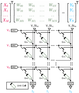
The image depicts a block diagram of a linear system implementing matrix multiplication, represented by the equation **X<sup>T</sup>W = Y<sup>T</sup>**. The system uses a cascaded array of "Unit Cells" to process input voltages (**V₀, V₁, ..., Vₘ**) through resistor networks and analog-to-digital converters (ADCs) to generate output currents (**I₀, I₁, ..., Iₙ**).
### Components/Axes
1. **Matrix Equation**:
- **X**: Input vector with elements **X₀, X₁, ..., Xₘ** (transposed as a row vector).
- **W**: Weight matrix with elements **W<sub>ij</sub>** (e.g., **W₀₀, W₀₁, ..., Wₘₙ**).
- **Y**: Output vector with elements **Y₀, Y₁, ..., Yₙ** (transposed as a row vector).
- Equation: **X<sup>T</sup>W = Y<sup>T</sup>** implies **Y = WX** (standard matrix multiplication).
2. **Circuit Diagram**:
- **Input Voltages**: **V₀, V₁, ..., Vₘ** (labeled in red) connected to DACs (Digital-to-Analog Converters).
- **Resistor Network**: Labeled **G<sub>ij</sub>** (e.g., **G₀₀, G₀₁, ..., Gₘₙ**), representing conductances.
- **Voltage Sources**: **V_SL₀, V_SL₁, ..., V_SLₙ** (labeled in gray) applied to the top of each resistor column.
- **Unit Cells**: Repeated blocks containing DACs, resistors, and current summation paths.
- **Output Currents**: **I₀, I₁, ..., Iₙ** (labeled in blue) extracted via ADCs at the bottom.
### Detailed Analysis
- **Matrix Structure**:
- **X** is a **(m+1)×1** column vector.
- **W** is a **(m+1)×(n+1)** matrix (rows = m+1, columns = n+1).
- **Y** is a **(n+1)×1** column vector.
- Example: For **m=2, n=2**, **W** has 3 rows (W₀₀, W₁₀, W₂₀; W₀₁, W₁₁, W₂₁; W₀₂, W₁₂, W₂₂).
- **Circuit Flow**:
1. Input voltages (**V₀–Vₘ**) are converted to analog signals via DACs.
2. Each DAC output drives a column of resistors (**G<sub>ij</sub>**) connected to voltage sources (**V_SLⱼ**).
3. Currents flow through resistors, summing at the bottom of each column.
4. ADCs convert summed currents (**I₀–Iₙ**) to digital outputs.
### Key Observations
- **Resistor Network**: The **G<sub>ij</sub>** values determine the weighting of input voltages in the matrix multiplication.
- **Voltage Sources**: **V_SLⱼ** likely act as reference voltages to bias the resistor network.
- **ADC Placement**: ADCs are positioned to measure the total current from each resistor column, corresponding to **Yⱼ** in the matrix equation.
### Interpretation
This system implements a **linear transformation** (matrix multiplication) in analog hardware. The resistor network (**W**) scales and combines input voltages (**X**) to produce output currents (**Y**). The ADCs digitize these currents for further processing.
- **Technical Significance**:
- The circuit could function as a **current-steering DAC** or **analog filter**, where **W** defines the filter coefficients or transformation matrix.
- The use of DACs and ADCs suggests integration with digital control systems.
- **Design Constraints**:
- Resistor values (**G<sub>ij</sub>**) must be precisely matched to avoid errors in matrix multiplication.
- Voltage sources (**V_SLⱼ**) must be stable to ensure accurate current summation.
- **Anomalies**:
- No explicit grounding paths are shown for the voltage sources or ADCs, which could impact real-world implementation.
- The diagram assumes ideal DAC/ADC behavior (no noise or nonlinearity).
This design bridges analog and digital domains, enabling efficient matrix operations for applications like signal processing or machine learning accelerators.