\n
## Technical Diagram: Byte-Level Write Enable Control
### Overview
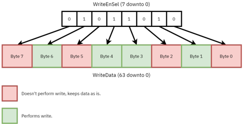
This image is a technical diagram illustrating a digital control mechanism for selective byte writing in a 64-bit data word. It shows how an 8-bit control signal (`WriteEnSel`) determines which of the 8 bytes in a 64-bit data bus (`WriteData`) will be written to memory or a register, and which will retain their existing values.
### Components/Axes
The diagram is structured into three main regions:
1. **Header / Control Signal (Top):**
* **Label:** `WriteEnSel (7 downto 0)`
* **Content:** An 8-bit register or bus represented as a row of 8 boxes.
* **Bit Values (from left to right, corresponding to bit 7 down to bit 0):** `0`, `1`, `0`, `1`, `1`, `0`, `1`, `0`.
2. **Main Data Path (Center):**
* **Label:** `WriteData (63 downto 0)`
* **Content:** A 64-bit data bus divided into 8 distinct byte-sized blocks.
* **Byte Labels (from left to right):** `Byte 7`, `Byte 6`, `Byte 5`, `Byte 4`, `Byte 3`, `Byte 2`, `Byte 1`, `Byte 0`.
* **Color Coding:** The bytes are colored either red or green, corresponding to the control logic defined in the legend.
* **Flow/Connection:** Black arrows originate from each individual bit box in the `WriteEnSel` row and point directly to the corresponding byte block below. The arrow from bit `n` points to `Byte n`.
3. **Footer / Legend (Bottom-Left):**
* A legend box explaining the color-coding scheme.
* **Red Square:** Label: `Doesn't perform write, keeps data as is.`
* **Green Square:** Label: `Performs write.`
### Detailed Analysis
The diagram defines a precise, bit-for-byte control relationship:
* **Control Signal (`WriteEnSel`) Bit Mapping:**
* Bit 7 = `0` → Controls `Byte 7`
* Bit 6 = `1` → Controls `Byte 6`
* Bit 5 = `0` → Controls `Byte 5`
* Bit 4 = `1` → Controls `Byte 4`
* Bit 3 = `1` → Controls `Byte 3`
* Bit 2 = `0` → Controls `Byte 2`
* Bit 1 = `1` → Controls `Byte 1`
* Bit 0 = `0` → Controls `Byte 0`
* **Data Path (`WriteData`) Byte Status (Based on Color & Legend):**
* `Byte 7`: **Red** → Does not perform write. Data remains unchanged.
* `Byte 6`: **Green** → Performs write. Data is updated.
* `Byte 5`: **Red** → Does not perform write. Data remains unchanged.
* `Byte 4`: **Green** → Performs write. Data is updated.
* `Byte 3`: **Green** → Performs write. Data is updated.
* `Byte 2`: **Red** → Does not perform write. Data remains unchanged.
* `Byte 1`: **Green** → Performs write. Data is updated.
* `Byte 0`: **Red** → Does not perform write. Data remains unchanged.
* **Logic Verification:** The color of each byte block perfectly matches the value of its controlling bit in `WriteEnSel`. A control bit value of `1` results in a green (write) byte, and a value of `0` results in a red (no-write) byte.
### Key Observations
1. **Selective Write Pattern:** The control signal `0b01011010` (binary) or `0x5A` (hexadecimal) enables writes to the even-numbered bytes (6, 4, 3, 1) while disabling writes to the odd-numbered bytes (7, 5, 2, 0). *Note: Byte numbering is 0-indexed from the right.*
2. **Spatial Layout:** The legend is positioned in the bottom-left corner, separate from the main flow. The control register is centered at the top, and the data bus is centered below it, with a clear, direct mapping via arrows.
3. **Visual Clarity:** The use of color (red/green) and direct arrows creates an unambiguous, at-a-glance understanding of which data bytes are active for a write operation based on the control bits.
### Interpretation
This diagram is a classic representation of a **byte write enable** or **byte lane write control** scheme, fundamental in computer architecture and digital design.
* **Function:** It allows a system to perform **partial writes** to a wider data word (64 bits here). Instead of always writing all 8 bytes, the system can update only the specific bytes needed. This is crucial for efficiency, reducing power consumption, and preventing unnecessary modification of data.
* **Underlying Principle:** The `WriteEnSel` register acts as a **mask**. Each bit in the mask corresponds to a byte lane in the data bus. A '1' in the mask "opens the gate" for that byte's data to be written, while a '0' "closes the gate," preserving the existing value in the destination memory or register.
* **Application Context:** This mechanism is commonly used in memory controllers, bus interfaces (like AXI or Wishbone), and CPU load/store units. For example, when a processor writes a 32-bit integer to an address that is not aligned to a 64-bit boundary, only the relevant bytes within the 64-bit bus would be enabled for writing.
* **Data Inference:** The specific pattern shown (`01011010`) is likely an example for illustration. In a real system, this value would be generated dynamically by control logic based on the size and alignment of the data being written.