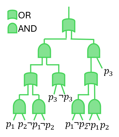
## Logic Gate Diagram: Hierarchical Boolean Expression Structure
### Overview
The image depicts a hierarchical logic gate circuit composed of AND, OR, and NOT gates. The diagram uses green-colored gates with standardized symbols: rectangles for AND gates, inverted triangles for NOT gates, and horizontal lines for connections. The structure forms a tree-like hierarchy with inputs at the base and a single output at the top.
### Components/Axes
- **Legend**:
- Top-left corner contains a green square labeled "OR" and a green semicircle labeled "AND"
- No explicit NOT gate symbol in legend, but inverted triangle shapes are used throughout
- **Gates**:
- **Top Level**: Single OR gate (rectangle) at apex
- **Second Level**: Two AND gates (rectangles) connected to OR gate
- **Third Level**: Four AND gates (rectangles) connected to second-level AND gates
- **Fourth Level**: Eight NOT gates (inverted triangles) at base
- **Inputs**:
- Labeled p1, p2, p3 at NOT gate inputs
- Connections show inverted signals (p1̄, p2̄, p3̄)
- **Outputs**:
- Intermediate AND gate outputs labeled:
- "p3 AND p3" (right branch)
- "p1 AND p2" (left branch)
- Final OR gate output not explicitly labeled
### Detailed Analysis
1. **Gate Connections**:
- Top OR gate receives inputs from:
- Right AND gate (output: p3 AND p3)
- Left AND gate (output: p1 AND p2)
- Second-level AND gates receive inverted inputs:
- Right AND: p3̄ AND p3̄
- Left AND: p1̄ AND p2̄
- Third-level AND gates process:
- Right branch: p1̄ AND p2̄ AND p1 AND p2
- Left branch: p3̄ AND p3̄ AND p3 AND p3
2. **Signal Flow**:
- Inputs (p1, p2, p3) enter NOT gates at base
- Inverted signals (p1̄, p2̄, p3̄) combine with original signals in AND gates
- AND gate outputs combine at higher levels
- Final OR gate combines top-level AND outputs
### Key Observations
- **Redundant Operations**:
- p3 AND p3 simplifies to p3
- p1 AND p2 AND p1 AND p2 simplifies to p1 AND p2
- **Symmetry**:
- Left and right branches mirror each other in structure
- Both branches use identical gate configurations
- **Signal Inversion**:
- All inputs pass through NOT gates before AND operations
- Creates complementary signal paths
### Interpretation
This diagram represents a complex boolean expression:
`(p1 AND p2) OR (p3 AND p3)`
Which simplifies to:
`(p1 AND p2) OR p3`
The hierarchical structure demonstrates:
1. **Signal Processing**: Inputs are inverted before combination
2. **Redundancy Elimination**: Duplicate AND operations simplify to single variables
3. **Logical Prioritization**: OR gate at top level determines final output
The circuit appears designed to implement a specific boolean function with potential applications in digital logic design, where:
- p1 AND p2 represents a primary condition
- p3 acts as an independent enabling condition
- The OR gate at top level creates a fail-safe mechanism where either condition can trigger the output