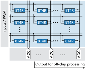
## Block Diagram: 8T4R Array with ADC Outputs
### Overview
The diagram illustrates a structured array of 8T4R (8 Transistor, 4 Resistor) blocks organized in a grid format. Each block is interconnected with horizontal and vertical lines, suggesting signal routing or data flow. At the bottom of the grid, multiple ADC (Analog-to-Digital Converter) labels are positioned, with an arrow indicating "Output for off-chip processing." The left side of the diagram is labeled "Inputs / PWM," implying input signals or pulse-width modulation sources.
### Components/Axes
- **Grid Structure**:
- Rows and columns of 8T4R blocks (exact count unspecified, represented by ellipses).
- Each 8T4R block is a blue rectangular component with white text.
- **Labels**:
- **Left Side**: "Inputs / PWM" (vertical orientation).
- **Bottom**: "Output for off-chip processing" (horizontal arrow pointing right).
- **ADC Labels**: Repeated "ADC" labels at the bottom, spaced evenly (exact count unspecified, represented by ellipses).
- **Connections**:
- Black lines connect 8T4R blocks horizontally and vertically, forming a matrix-like network.
- Vertical lines on the far left and right edges of the grid suggest input/output pathways.
### Detailed Analysis
- **8T4R Blocks**:
- Arranged in a grid with at least 3 visible rows and 3 visible columns (ellipses indicate continuation).
- Each block is identical in labeling ("8T4R") and connected to adjacent blocks via horizontal and vertical lines.
- **ADC Outputs**:
- ADC labels are positioned at the bottom of the grid, aligned with the 8T4R blocks.
- The arrow labeled "Output for off-chip processing" suggests data from the ADCs is routed externally.
- **Input/Output Flow**:
- "Inputs / PWM" on the left implies signals enter the grid from the left side.
- The grid processes these signals through the 8T4R blocks, which then route data to the ADCs at the bottom.
### Key Observations
- The grid’s repetitive 8T4R blocks suggest a modular or parallel processing architecture.
- The absence of numerical values or explicit scaling indicates the diagram focuses on structural relationships rather than quantitative data.
- The ADC labels and off-chip output arrow imply the system’s purpose is signal conversion and external data transmission.
### Interpretation
This diagram likely represents a hardware architecture for signal processing, where:
1. **Inputs** (PWM or analog signals) enter the system and are processed through a matrix of 8T4R blocks.
2. The 8T4R blocks may perform functions like amplification, filtering, or modulation, given their transistor-resistor configuration.
3. Processed signals are converted to digital via ADCs and sent for off-chip processing (e.g., computation, storage, or communication).
4. The grid structure emphasizes scalability, with ellipses suggesting the system can expand horizontally/vertically.
The diagram does not provide numerical data, so trends or quantitative analysis are not applicable. The focus is on the logical flow of signals through the hardware components.