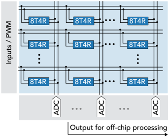
## Diagram: Crossbar Array Architecture
### Overview
The image depicts a crossbar array architecture, likely used in a memory or processing system. It shows a grid of interconnected cells, with inputs/PWM signals on one side and ADC outputs on the other.
### Components/Axes
* **Inputs/PWM:** Label on the left side, indicating input signals or Pulse Width Modulation.
* **ADC:** Label at the bottom, indicating Analog-to-Digital Converter outputs.
* **8T4R:** Label within each cell of the array, likely representing an 8-Transistor 4-Resistor memory cell.
* **Dots (...):** Indicate continuation of the array structure in both horizontal and vertical directions.
* **Output for off-chip processing:** Label with an arrow pointing to the right, indicating the destination of the ADC outputs.
### Detailed Analysis
The diagram shows a 3x3 grid of cells, each labeled "8T4R". The cells are interconnected by horizontal and vertical lines. The horizontal lines are connected to "Inputs/PWM" on the left. The vertical lines are connected to "ADC" at the bottom. The dots indicate that the array extends beyond the visible portion.
### Key Observations
* The array structure is regular and repetitive.
* The "8T4R" cells are the fundamental building blocks of the array.
* The "Inputs/PWM" signals are converted to digital signals by the "ADC" and sent for off-chip processing.
### Interpretation
The diagram illustrates a crossbar array architecture, which is a common structure for memory and processing systems. The "8T4R" cells likely store or process data. The "Inputs/PWM" signals are used to write data to the cells or control their operation. The "ADC" converts the analog signals from the cells to digital signals, which can be processed by external circuitry. The use of "off-chip processing" suggests that the array is part of a larger system.