TECHNICAL ASSET FINGERPRINT
d3f4b14f88b8fc5c2511fc7f
Click to view fullscreen
Press ESC or click to close
FOUND IN PAPERS
EXPERT: healer-alpha-free VERSION 1
RUNTIME: free/openrouter/healer-alpha
INTEL_VERIFIED
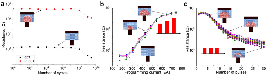
## [Multi-Panel Scientific Chart]: Resistance Switching Characteristics of a Memristive Device
### Overview
The image is a composite figure containing three subplots (labeled **a**, **b**, and **c**) that characterize the resistive switching behavior of a device, likely a memristor or resistive random-access memory (ReRAM) cell. The plots show how electrical resistance changes in response to cycling, programming current, and voltage pulses. Each plot includes schematic diagrams illustrating the proposed state of the conductive filament within the device at different stages.
### Components/Axes
The figure is divided into three distinct panels arranged horizontally.
**Panel a (Left):**
* **Title/Label:** "a" (top-left corner).
* **Y-axis:** Label: "Resistance (Ω)". Scale: Logarithmic, ranging from 10⁴ to 10⁷ Ω.
* **X-axis:** Label: "Number of cycles". Scale: Logarithmic, ranging from 10⁰ to 10¹⁰ cycles.
* **Legend:** Located in the bottom-left corner. Contains two entries:
* Black square symbol: "SET"
* Red circle symbol: "RESET"
* **Embedded Diagrams:** Two schematic cross-sections of a device structure (top electrode, switching layer with red dots representing a conductive filament, bottom electrode). Arrows point from specific data points to these diagrams, indicating the filament state corresponding to that resistance level.
**Panel b (Center):**
* **Title/Label:** "b" (top-left corner).
* **Y-axis:** Label: "Resistance (Ω)". Scale: Logarithmic, ranging from 10⁵ to 10⁷ Ω.
* **X-axis:** Label: "Programming current (µA)". Scale: Linear, ranging from 100 to 800 µA.
* **Legend:** No explicit legend box. Multiple data series are plotted with different colored symbols (purple squares, blue circles, green diamonds, etc.). Each color is linked via an arrow to a specific schematic diagram of the device filament.
* **Embedded Diagrams:** Four schematic diagrams showing different filament morphologies (from small/weak to large/strong). Arrows connect these diagrams to specific data series/points on the plot.
* **Inset Bar Chart:** Located in the bottom-right quadrant. Shows three red vertical bars of increasing height. An arrow points from this bar chart to the main plot's x-axis, suggesting it represents discrete current steps or levels used in an experiment.
**Panel c (Right):**
* **Title/Label:** "c" (top-left corner).
* **Y-axis:** Label: "Resistance (Ω)". Scale: Logarithmic, ranging from 10⁵ to 10⁷ Ω.
* **X-axis:** Label: "Number of pulses". Scale: Linear, ranging from 0 to 30 pulses.
* **Legend:** No explicit legend box. Multiple data series are plotted with different colored symbols (purple, blue, green, etc.), similar to panel b.
* **Embedded Diagrams:** Three schematic diagrams showing the progressive dissolution or weakening of a conductive filament. Arrows connect these diagrams to different regions of the decaying resistance curves.
* **Inset Bar Chart:** Located in the bottom-left quadrant. Shows three red vertical bars of equal height. An arrow points from this bar chart to the main plot's x-axis, suggesting it represents the application of a constant-amplitude pulse train.
### Detailed Analysis
**Panel a: Endurance Cycling**
* **Trend Verification:** The **SET state (black squares)** shows a relatively stable, high resistance (~1.5 x 10⁴ Ω) from 1 cycle up to approximately 10⁸ cycles, after which it begins a gradual decline, dropping below 10⁴ Ω by 10¹⁰ cycles. The **RESET state (red circles)** maintains a very high resistance (~5 x 10⁶ Ω) consistently from 1 cycle to about 10⁸ cycles. After 10⁸ cycles, the RESET resistance also begins to decrease, falling to ~1-2 x 10⁶ Ω by 10¹⁰ cycles.
* **Data Points (Approximate):**
* RESET @ 1 cycle: ~5 x 10⁶ Ω
* SET @ 1 cycle: ~1.5 x 10⁴ Ω
* RESET @ 10⁸ cycles: ~5 x 10⁶ Ω
* SET @ 10⁸ cycles: ~1.5 x 10⁴ Ω
* RESET @ 10¹⁰ cycles: ~1.5 x 10⁶ Ω
* SET @ 10¹⁰ cycles: ~8 x 10³ Ω
* **Embedded Diagram Context:** The diagram linked to the high RESET resistance shows a thick, robust conductive filament (many red dots). The diagram linked to the lower SET resistance shows a thinner, possibly constricted filament.
**Panel b: Current-Dependent Switching**
* **Trend Verification:** All data series show a strong positive correlation between programming current and the resulting resistance state. As the programming current increases from ~200 µA to ~700 µA, the resistance increases by approximately two orders of magnitude (from ~10⁵ Ω to ~10⁷ Ω). The curves have a sigmoidal shape, with a steep transition region between 300 µA and 500 µA.
* **Data Points & Series (Approximate):**
* At ~200 µA: All series cluster between 2 x 10⁵ Ω and 5 x 10⁵ Ω.
* At ~400 µA (mid-transition): Series are spread between 10⁶ Ω and 5 x 10⁶ Ω.
* At ~700 µA: Series converge near the top of the scale, between 5 x 10⁶ Ω and 10⁷ Ω.
* **Component Isolation (Diagrams):** The four diagrams are positioned around the plot. The bottom-left diagram (small filament) is linked to the low-resistance data at low current. The top-left diagram (medium filament) links to the transition region. The top-right diagram (large, dense filament) links to the high-resistance saturation region at high current. The bottom-right diagram (very large filament) is also linked to the high-current region.
**Panel c: Pulse-Induced Degradation**
* **Trend Verification:** All data series show a clear negative correlation, with resistance decaying as the number of applied pulses increases. The decay is rapid initially (first 5-10 pulses) and then gradually slows, approaching a lower asymptotic value. The overall drop is from ~5-6 x 10⁶ Ω to ~1-2 x 10⁵ Ω over 30 pulses.
* **Data Points & Series (Approximate):**
* Pulse 0 (Initial): All series start between 4 x 10⁶ Ω and 7 x 10⁶ Ω.
* Pulse 5: Resistance has dropped to between 1 x 10⁶ Ω and 3 x 10⁶ Ω.
* Pulse 15: Resistance is between 3 x 10⁵ Ω and 8 x 10⁵ Ω.
* Pulse 30: Final resistance values range from ~1 x 10⁵ Ω to ~3 x 10⁵ Ω.
* **Component Isolation (Diagrams):** The top-left diagram (intact filament) corresponds to the high initial resistance. The middle-right diagram (partially dissolved filament) corresponds to the mid-decay region. The bottom-right diagram (severely dissolved/broken filament) corresponds to the low final resistance state.
### Key Observations
1. **High Endurance:** The device in panel **a** demonstrates stable switching for up to 10⁸ cycles before significant degradation begins.
2. **Analog Switching:** Panel **b** shows that the final resistance state is not binary but can be analogically tuned by the magnitude of the programming current.
3. **Pulse-Induced State Change:** Panel **c** demonstrates that applying a series of identical pulses can gradually and controllably reduce the device resistance, suggesting a mechanism for potentiation or depression in neuromorphic contexts.
4. **Filamentary Mechanism:** The consistent use of embedded diagrams showing a conductive filament (red dots) that grows, shrinks, or dissolves strongly indicates that the resistive switching is governed by the formation and rupture of a metallic conductive filament within the insulating layer.
### Interpretation
This figure collectively characterizes a memristive device's performance and underlying physical mechanism. **Panel a** establishes its reliability and longevity for memory applications. **Panel b** reveals its potential for multi-level cell storage or analog computing, where the "strength" of the stored state (resistance) is a function of the writing energy (current). **Panel c** is particularly significant for neuromorphic engineering, as it mimics synaptic plasticity—the gradual weakening of a connection (synaptic weight, represented here by conductance, the inverse of resistance) with repeated stimulation (pulses). The embedded diagrams provide a Peircean *iconic* representation, linking the abstract electrical data to a hypothesized physical structure (the filament), making the proposed mechanism of operation clear. The degradation after 10⁸ cycles in panel **a** is a critical reliability metric, indicating the device's operational lifetime. The tight correlation between the visual state of the filament in the diagrams and the measured electrical data across all three panels strongly supports the filamentary switching model for this device.
DECODING INTELLIGENCE...