\n
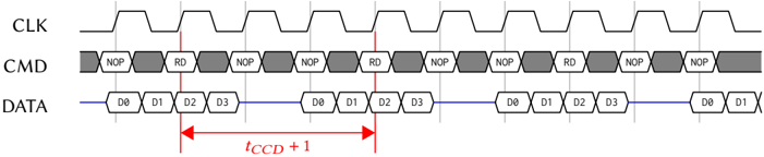
## Diagram: Timing Diagram for Read Operation
### Overview
This diagram illustrates the timing relationship between the Clock (CLK), Command (CMD), and Data signals during a read operation. It depicts a sequence of NOP (No Operation) and RD (Read) commands interleaved with data transfer. The diagram highlights the timing constraint `tCCD + 1`.
### Components/Axes
The diagram consists of three horizontal signal traces:
* **CLK:** Clock signal, represented as a square wave.
* **CMD:** Command signal, showing a repeating pattern of NOP and RD commands.
* **DATA:** Data signal, showing data values D0, D1, D2, and D3 being transferred.
* **tCCD + 1:** A timing annotation indicating a duration measured in clock cycles.
### Detailed Analysis
The diagram shows a repeating pattern. Let's analyze the timing:
* **CLK:** The clock signal is periodic with a consistent pulse width and period.
* **CMD:** The command signal alternates between NOP (represented by light gray blocks) and RD (represented by dark gray blocks). Each RD command is preceded and followed by NOP commands.
* **DATA:** The data signal shows data values D0, D1, D2, and D3 being presented on the data bus during the RD command. The data appears to be valid during the rising edge of the clock signal following the RD command.
* **Timing Annotation:** The annotation `tCCD + 1` is indicated by a red double-arrow spanning several clock cycles. It starts at the rising edge of the clock signal that triggers the RD command and extends to the rising edge of the clock signal after the last data value (D3) is presented. The length of `tCCD + 1` appears to be approximately 5 clock cycles.
### Key Observations
* The read operation requires a specific timing relationship between the command and data signals.
* The `tCCD + 1` parameter defines the minimum time required for the data to be valid after issuing the read command.
* The diagram shows a synchronous data transfer, where data is transferred on the rising edge of the clock.
* The data is presented in a sequential manner (D0, D1, D2, D3).
### Interpretation
This timing diagram demonstrates the protocol for reading data from a memory or peripheral device. The `tCCD + 1` parameter is crucial for ensuring data integrity. It represents the time needed for the device to respond to the read command and present valid data on the data bus. The alternating NOP and RD commands suggest a pipelined or interleaved operation, where the device can process commands while data is being transferred. The diagram is a simplified representation and likely omits details such as address signals or control signals. The diagram suggests a relatively slow data transfer rate, as it takes multiple clock cycles to transfer a small amount of data (4 bits). The diagram is a critical component of a technical specification, defining the precise timing requirements for a successful read operation.