## Timing Diagram: Memory Read Command Sequence with t_CCD Parameter
### Overview
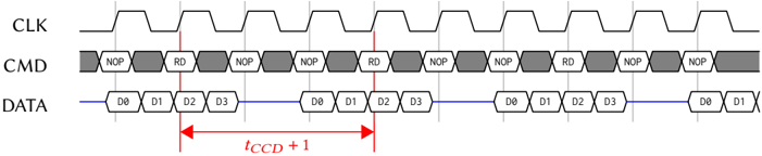
The image is a digital timing diagram illustrating the relationship between a clock signal (CLK), command signals (CMD), and data signals (DATA) in a synchronous memory interface. It specifically highlights the timing parameter `t_CCD + 1` (CAS-to-CAS Delay) between consecutive read (RD) commands.
### Components/Axes
The diagram is organized into three horizontal signal rows, aligned vertically by time:
1. **CLK (Top Row):** A continuous square wave clock signal. It has no explicit axis labels but serves as the fundamental timing reference.
2. **CMD (Middle Row):** A command bus showing a sequence of operations. The visible commands are:
* `NOP` (No Operation)
* `RD` (Read)
The sequence from left to right is: `NOP`, `RD`, `NOP`, `NOP`, `RD`, `NOP`, `NOP`, `RD`, `NOP`, `RD`.
3. **DATA (Bottom Row):** A data bus showing the output of read operations. Data packets are labeled:
* `D0`, `D1`, `D2`, `D3` (First burst)
* `D0`, `D1`, `D2`, `D3` (Second burst)
* `D0`, `D1`, `D2`, `D3` (Third burst)
* `D0`, `D1` (Partial fourth burst visible)
4. **Timing Annotation:** A red, double-headed arrow labeled `t_CCD + 1` is positioned below the DATA line. It spans from the rising clock edge where the first `RD` command is issued to the rising clock edge where the second `RD` command is issued. Two vertical red lines mark these start points.
### Detailed Analysis
* **Command Sequence:** The diagram shows three complete read (`RD`) operations. Each `RD` command is preceded and followed by one or more `NOP` commands, which are used to insert idle cycles and manage timing.
* **Data Output:** Each `RD` command initiates a burst of four data words (`D0` through `D3`). The data appears on the DATA bus with a fixed latency after the corresponding `RD` command. For example, the first `D0` appears several clock cycles after the first `RD`.
* **Timing Parameter (`t_CCD + 1`):** This is the critical extracted data point. The annotation defines the interval between the initiation of two consecutive read commands.
* **Start Point:** The rising edge of the clock cycle where the first `RD` command is active.
* **End Point:** The rising edge of the clock cycle where the second `RD` command is active.
* **Value:** The parameter is expressed as `t_CCD + 1`. This indicates the actual delay is one clock cycle longer than the base `t_CCD` timing specification of the memory device. Visually, there are **5 full clock cycles** between the two marked rising edges.
### Key Observations
1. **Fixed Latency:** The time from an `RD` command to the start of its corresponding data burst (`D0`) appears consistent across all three read operations.
2. **Burst Length:** The memory is configured for a burst length of 4, as each `RD` command yields four consecutive data words (`D0-D3`).
3. **NOP Insertion:** The number of `NOP` cycles between `RD` commands is not constant. Between the first and second `RD`, there are two `NOP` cycles. Between the second and third `RD`, there are also two `NOP` cycles. This spacing is dictated by the `t_CCD + 1` timing requirement.
4. **Spatial Grounding:** The red timing annotation is placed in the lower portion of the diagram, spanning the horizontal space between the first and second `RD` command markers. Its endpoints are precisely aligned with the vertical red lines that intersect the CLK and CMD signals at the relevant command start points.
### Interpretation
This diagram is a technical specification for memory controller design. It demonstrates how to schedule read commands to a memory chip (like DDR SDRAM) while respecting the `t_CCD` timing parameter.
* **What it means:** `t_CCD` is the minimum time interval required between two column-access (read or write) commands. The diagram shows a practical implementation where the controller must wait `t_CCD + 1` clock cycles between issuing consecutive `RD` commands. The "+1" likely accounts for internal pipeline delays or a specific operating mode.
* **Why it matters:** Violating this timing parameter (by issuing `RD` commands too close together) would lead to data corruption, bus contention, or system failure. The `NOP` commands are essential "filler" to enforce this delay.
* **Underlying Pattern:** The diagram reveals a deterministic, pipelined system. Commands are issued on a strict schedule, and data follows with a fixed, predictable latency. The varying number of `NOP`s between commands (though constant in this example) shows how the controller dynamically inserts idle cycles to meet different timing constraints (`t_CCD`, `tRCD`, `tRP`, etc.) in a real memory access sequence.