## DRAM Rank Attack Mitigation Diagram
### Overview
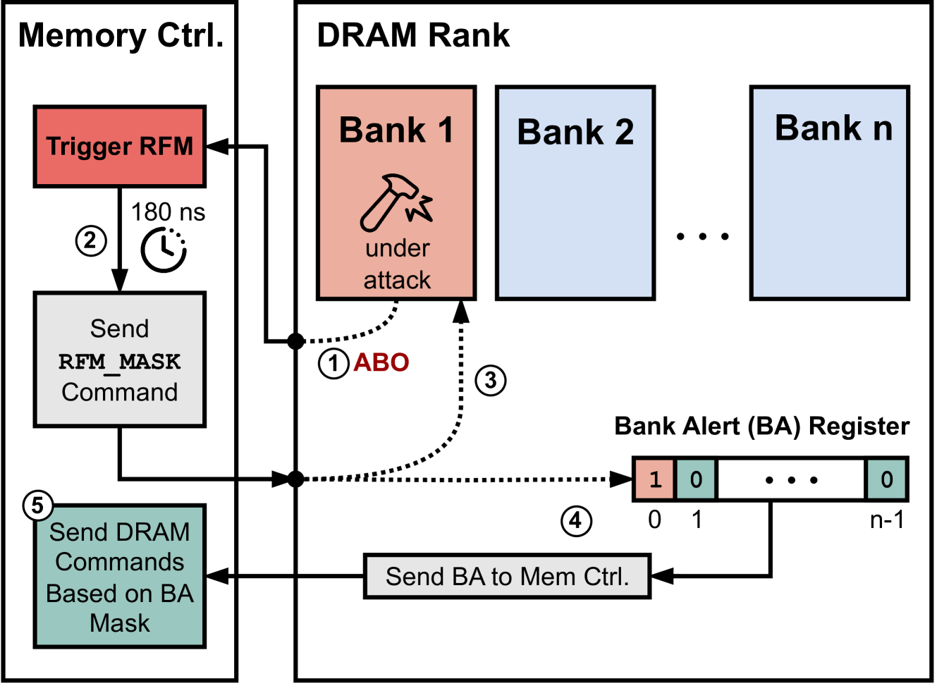
The image is a diagram illustrating a DRAM rank attack mitigation process. It shows the interaction between the Memory Controller (Memory Ctrl.) and the DRAM Rank, highlighting the steps involved in detecting and responding to an attack on a specific bank within the DRAM.
### Components/Axes
* **Memory Ctrl.:** Represents the memory controller unit.
* **Trigger RFM:** A red block within the Memory Ctrl., presumably triggering a refresh mechanism.
* **Send RFM\_MASK Command:** A gray block, indicating a command is sent.
* **Send DRAM Commands Based on BA Mask:** A light green block, indicating DRAM commands are sent based on a Bank Alert mask.
* **DRAM Rank:** Represents the DRAM memory rank.
* **Bank 1:** A red block, labeled "Bank 1," indicating it is under attack, symbolized by a hammer icon.
* **Bank 2:** A light blue block, labeled "Bank 2."
* **Bank n:** A light blue block, labeled "Bank n."
* **Bank Alert (BA) Register:** A register containing bits representing the alert status of each bank. The first bit (index 0) is set to 1 (red), indicating an alert, while the second bit (index 1) is set to 0 (light green), and the last bit (index n-1) is set to 0 (light green).
* **Arrows and Labels:**
* **(1) ABO:** Indicates the Address Bit Offset.
* **(2):** Indicates a delay of 180 ns.
* **(3):** Indicates the path from the attacked bank to the Bank Alert Register.
* **(4):** Indicates the path from the Bank Alert Register to "Send BA to Mem Ctrl."
* **(5):** Indicates the path from "Send BA to Mem Ctrl." to "Send DRAM Commands Based on BA Mask."
### Detailed Analysis
1. **Attack Initiation:** Bank 1 is shown "under attack," indicated by a hammer icon.
2. **Address Bit Offset (ABO):** The attack on Bank 1 triggers an Address Bit Offset (ABO) event, labeled as step (1).
3. **Trigger RFM:** The ABO event triggers the "Trigger RFM" block in the Memory Controller.
4. **Delay:** There is a 180 ns delay (step 2) after triggering RFM.
5. **Send RFM\_MASK Command:** After the delay, the Memory Controller sends an RFM\_MASK command.
6. **Bank Alert Register Update:** The attack on Bank 1 causes the corresponding bit in the Bank Alert (BA) Register to be set to 1 (step 3). The register is indexed from 0 to n-1, with the first bit (index 0) set to 1, indicating Bank 1 is under attack.
7. **Send BA to Mem Ctrl.:** The Bank Alert Register sends the BA information to the Memory Controller (step 4).
8. **Send DRAM Commands Based on BA Mask:** The Memory Controller then sends DRAM commands based on the BA mask (step 5).
### Key Observations
* The diagram illustrates a closed-loop system where an attack on a DRAM bank triggers a response from the Memory Controller.
* The Bank Alert Register plays a crucial role in identifying and masking the affected bank.
* The RFM (Refresh Mechanism) is triggered as part of the mitigation process.
### Interpretation
The diagram depicts a mechanism for mitigating attacks on DRAM by using a Bank Alert Register to identify compromised banks and trigger appropriate responses from the Memory Controller. The process involves detecting the attack, setting the corresponding bit in the Bank Alert Register, and then using this information to mask the affected bank when sending DRAM commands. This helps to isolate the attack and prevent it from spreading to other parts of the memory system. The 180 ns delay suggests a time window for attack detection and response initiation. The use of RFM suggests that refreshing the memory is part of the mitigation strategy, potentially to clear corrupted data.