\n
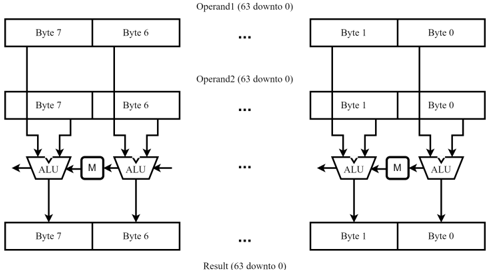
## Diagram: Byte-Level ALU Processing Architecture
### Overview
The image is a technical block diagram illustrating a parallel processing architecture for 64-bit operands. It depicts how two 64-bit input operands (Operand1 and Operand2) are processed byte-by-byte through a series of Arithmetic Logic Units (ALUs) to produce a 64-bit result. The diagram emphasizes a data flow from top to bottom, with horizontal connections between processing elements.
### Components/Axes
The diagram is structured into three primary horizontal rows, with vertical data flow:
1. **Top Row (Input Operands):**
* **Operand1 (63 downto 0):** A 64-bit input, visually segmented into 8 bytes. The leftmost byte is labeled "Byte 7" and the rightmost is "Byte 0". An ellipsis ("...") indicates the continuation of bytes between Byte 6 and Byte 1.
* **Operand2 (63 downto 0):** A second 64-bit input, identically segmented and labeled as Operand1, positioned directly below it.
2. **Middle Row (Processing Elements):**
* This row contains a series of processing blocks. For each byte position (from 7 down to 0), there is a pair of components:
* **ALU:** An Arithmetic Logic Unit, represented by a trapezoidal block. It receives two inputs: one from the corresponding byte of Operand1 and one from the corresponding byte of Operand2.
* **M:** A block labeled "M" (likely representing a Multiplexer, Memory, or control unit). It is positioned between adjacent ALUs (e.g., between the ALU for Byte 7 and the ALU for Byte 6). Arrows connect the ALUs to the "M" block, suggesting inter-byte communication or control.
* The pattern repeats for all byte positions, with ellipses ("...") indicating the continuation between the Byte 6/Byte 1 sections.
3. **Bottom Row (Output Result):**
* **Result (63 downto 0):** A 64-bit output, segmented and labeled identically to the input operands. Arrows point from each ALU down to its corresponding byte in the Result.
**Spatial Layout:**
* The legend/labels for the operands and result are centered above and below their respective rows.
* The processing elements (ALUs and M blocks) are arranged in a linear, horizontal array in the center of the diagram.
* Data flow is primarily vertical (from operands down through ALUs to the result), with secondary horizontal connections between ALUs via the "M" blocks.
### Detailed Analysis
* **Data Flow:** The diagram shows a clear, synchronous data path. For each byte position `i` (where `i` = 7, 6, ..., 0):
1. Byte `i` from Operand1 and Byte `i` from Operand2 are fed as inputs into the ALU at that position.
2. The ALU performs an operation (the specific operation is not defined in the diagram).
3. The output of the ALU is written to Byte `i` of the Result.
* **Inter-ALU Communication:** The "M" blocks create a horizontal chain between the ALUs. Arrows point from an ALU into the "M" block to its right, and from that "M" block into the ALU to its right. This structure is characteristic of a **carry chain** in an adder or a similar propagation path for status flags in a parallel processing unit.
* **Bit-Width Notation:** The labels "(63 downto 0)" use hardware description language (HDL) syntax, indicating a 64-bit bus where bit 63 is the most significant bit (MSB) and bit 0 is the least significant bit (LSB). The byte segmentation (Byte 7 to Byte 0) corresponds to this, with Byte 7 containing bits 63-56 and Byte 0 containing bits 7-0.
### Key Observations
1. **Parallel, Byte-Sliced Architecture:** The design processes all 8 bytes of the operands simultaneously in dedicated hardware, which is a hallmark of **SIMD (Single Instruction, Multiple Data)** or vector processing.
2. **Carry/Control Propagation:** The "M" blocks and their connecting arrows are a critical feature. They indicate that the processing of one byte is not entirely independent of its neighbors. This is essential for operations like addition where a carry from a lower byte must propagate to a higher byte.
3. **Uniform Structure:** The diagram is perfectly regular, with identical hardware replicated for each byte slice. This suggests a scalable design.
### Interpretation
This diagram is a high-level representation of a **64-bit, byte-sliceable ALU array**, likely part of a CPU's execution unit or a specialized co-processor. Its primary purpose is to illustrate the **microarchitecture** of how a wide arithmetic or logical operation is broken down into parallel, smaller operations with a mechanism for inter-slice communication.
* **What it demonstrates:** It shows the trade-off between parallelism and dependency. While the byte-level ALUs allow for parallel computation, the "M" chain (carry chain) introduces a sequential dependency that can limit the maximum operating frequency. The length of this chain (8 stages for 64 bits) is a key design parameter affecting performance.
* **Relationship between elements:** The operands are the source, the ALU array is the computational engine, the "M" chain is the critical path for data dependency, and the result is the sink. The diagram abstracts away control logic, focusing purely on the data path.
* **Notable implication:** The explicit depiction of the "M" chain suggests this diagram is intended for an audience concerned with performance analysis, timing, or hardware implementation, as it highlights the primary source of latency in the operation. The absence of specific ALU operation labels (e.g., ADD, AND) indicates the diagram is meant to be generic, applicable to various operations that use such a structure.