\n
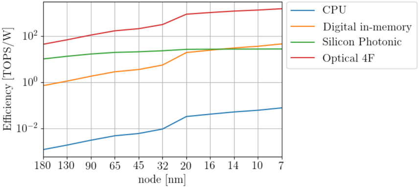
## Line Chart: Efficiency vs. Fabrication Node Size for Computing Technologies
### Overview
The image is a line chart comparing the computational efficiency, measured in Tera Operations Per Second per Watt (TOPS/W), of four different computing technologies across a range of semiconductor fabrication node sizes (in nanometers). The chart uses a logarithmic scale for the y-axis (Efficiency) and a categorical, non-linear scale for the x-axis (node size), progressing from larger to smaller nodes.
### Components/Axes
* **X-Axis (Horizontal):** Labeled "node [nm]". It lists discrete semiconductor fabrication node sizes in descending order: 180, 130, 90, 65, 45, 32, 20, 16, 14, 10, 7.
* **Y-Axis (Vertical):** Labeled "Efficiency [TOPS/W]". It is a logarithmic scale with major grid lines at 10⁻² (0.01), 10⁰ (1), and 10² (100).
* **Legend:** Positioned in the top-right corner, outside the main plot area. It contains four entries, each with a colored line segment and a label:
* **Blue Line:** CPU
* **Orange Line:** Digital in-memory
* **Green Line:** Silicon Photonic
* **Red Line:** Optical 4F
### Detailed Analysis
The chart plots four data series, each showing a general upward trend in efficiency as the fabrication node size decreases (moves right on the x-axis).
1. **CPU (Blue Line):**
* **Trend:** Shows a steady, moderate upward slope. It is the lowest-performing technology across all nodes.
* **Approximate Data Points:**
* At 180 nm: ~0.001 TOPS/W
* At 32 nm: ~0.01 TOPS/W
* At 20 nm: ~0.04 TOPS/W
* At 7 nm: ~0.08 TOPS/W
2. **Digital in-memory (Orange Line):**
* **Trend:** Shows a strong upward slope, with a notable increase in the rate of improvement between 32 nm and 20 nm. It starts below the Silicon Photonic line but surpasses it around the 16 nm node.
* **Approximate Data Points:**
* At 180 nm: ~0.8 TOPS/W
* At 32 nm: ~4 TOPS/W
* At 20 nm: ~20 TOPS/W
* At 7 nm: ~50 TOPS/W
3. **Silicon Photonic (Green Line):**
* **Trend:** Shows a very gradual, almost flat upward slope. It starts as the second-most efficient technology but is overtaken by Digital in-memory at smaller nodes.
* **Approximate Data Points:**
* At 180 nm: ~10 TOPS/W
* At 32 nm: ~20 TOPS/W
* At 20 nm: ~25 TOPS/W
* At 7 nm: ~30 TOPS/W
4. **Optical 4F (Red Line):**
* **Trend:** Shows the steepest upward slope and the highest efficiency at all nodes. It demonstrates a dramatic increase in efficiency, especially between 32 nm and 20 nm.
* **Approximate Data Points:**
* At 180 nm: ~50 TOPS/W
* At 32 nm: ~200 TOPS/W
* At 20 nm: ~800 TOPS/W
* At 7 nm: ~1500 TOPS/W (estimated, as it extends beyond the 10² grid line).
### Key Observations
* **Performance Hierarchy:** There is a clear and consistent hierarchy in efficiency: Optical 4F > Digital in-memory ≈ Silicon Photonic > CPU. The gap between Optical 4F and the others is substantial, spanning roughly two orders of magnitude compared to CPU.
* **Impact of Node Scaling:** All technologies benefit from moving to smaller fabrication nodes, but the rate of benefit (the slope of the line) varies dramatically. Optical and Digital in-memory technologies show a much stronger positive correlation between node size reduction and efficiency gain compared to CPU and Silicon Photonic.
* **Crossover Point:** The "Digital in-memory" technology overtakes "Silicon Photonic" in efficiency somewhere between the 20 nm and 16 nm nodes, indicating a potential technological inflection point.
* **Logarithmic Scale:** The use of a logarithmic y-axis is crucial, as it allows the visualization of data spanning over five orders of magnitude (from ~0.001 to ~1500 TOPS/W) on a single chart.
### Interpretation
This chart illustrates a technological forecast or comparison suggesting that non-von Neumann computing architectures (like in-memory computing and photonic/optical computing) offer dramatically higher energy efficiency for computational tasks compared to traditional CPUs, and this advantage grows as semiconductor manufacturing advances.
The data implies that for future computing systems where power consumption is a critical constraint (e.g., in massive data centers, edge AI, or mobile devices), architectures like Optical 4F and Digital in-memory could become essential. The steep improvement curves for these technologies suggest they are not only more efficient but also scale more favorably with continued miniaturization (Moore's Law) than conventional silicon photonics or CPUs. The chart makes a strong case for continued research and investment into alternative computing paradigms to overcome the power efficiency limits of traditional processor designs.