## Diagram: Neural Network to Hardware Crossbar Mapping
### Overview
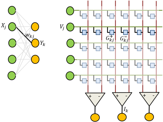
The image is a technical diagram illustrating the mapping between a conceptual artificial neural network layer (left) and its potential hardware implementation using a crossbar array (right), likely for analog or neuromorphic computing. It visually explains how synaptic weights are represented by programmable conductances in a physical circuit.
### Components/Axes
The diagram is divided into two primary, side-by-side sections:
**Left Section (Conceptual Neural Network):**
* **Input Layer:** Five green circles arranged vertically. The second circle from the top is labeled **`X_j`**.
* **Output Layer:** Three yellow circles arranged vertically.
* **Connections:** Gray lines connect every input node to every output node, representing a fully connected layer.
* **Highlighted Connection:** A single black line connects input node `X_j` to the top output node. This connection is labeled **`W_{kj}`**, representing the weight between input `j` and output `k`.
**Right Section (Hardware Crossbar Implementation):**
* **Input Lines (Rows):** Five horizontal green lines, each originating from a green circle (input neuron). The second line from the top is labeled **`V_j`**, representing the input voltage for neuron `j`.
* **Weight Elements (Synapses):** At each intersection of a horizontal input line and a vertical output line, there is a pair of blue squares. These represent programmable conductance elements (e.g., memristors, flash cells).
* The upper square in the pair is labeled **`G_{kj}^+`**.
* The lower square in the pair is labeled **`G_{kj}^-`**.
* This differential pair (`G^+` and `G^-`) allows the representation of both positive and negative weights.
* **Output Lines (Columns):** Three vertical red lines. Each line collects the summed current from all the conductance elements in its column.
* **Output Neurons/Circuits:** At the bottom of each red column line is a triangular symbol representing an operational amplifier or integrator.
* The amplifier has a **`+`** (non-inverting) input connected to the red column line and a **`-`** (inverting) input.
* The output of each amplifier is labeled **`I_k`**, representing the output current (or a voltage derived from it) for neuron `k`.
* Each `I_k` output is connected to a yellow circle, representing the output neuron.
### Detailed Analysis
The diagram establishes a direct component-to-component mapping:
1. **Input Transformation:** The conceptual input value `X_j` is translated into a physical input voltage `V_j` applied to a row in the crossbar.
2. **Weight Storage:** The abstract synaptic weight `W_{kj}` is implemented by the pair of conductances `G_{kj}^+` and `G_{kj}^-`. The effective weight is proportional to their difference (`G_{kj}^+ - G_{kj}^-`).
3. **Computation (Multiply-Accumulate):** The core computation happens at each crosspoint. The current through a conductance pair is `I = V_j * (G_{kj}^+ - G_{kj}^-)`. All currents from a column are summed by Kirchhoff's law onto the vertical red line.
4. **Output:** The summed column current is processed by the amplifier (which may also apply a nonlinear activation function) to produce the output signal `I_k` for the corresponding output neuron.
### Key Observations
* **Spatial Grounding:** The legend/labels (`G_{kj}^+`, `G_{kj}^-`) are placed directly next to their corresponding blue square components in the center of the crossbar grid. The input label `V_j` is at the left end of its row. The output label `I_k` is below its amplifier.
* **Component Isolation:** The diagram cleanly separates the abstract model (left) from the physical implementation (right), connected by the shared notation (`j`, `k` indices).
* **Trend/Flow Verification:** The flow is clearly from left (inputs) to right (crossbar) and then downward to the outputs. The black line `W_{kj}` on the left corresponds to the entire column of `G_{kj}^+`/`G_{kj}^-` pairs under the `k`-th output on the right.
* **Differential Pair:** The use of two conductances (`G^+` and `G^-`) per synapse is a critical detail for implementing signed weights in hardware that may only support positive conductance values.
### Interpretation
This diagram is a foundational illustration for the field of **neuromorphic engineering** or **in-memory computing**. It demonstrates how the core operation of a neural network—vector-matrix multiplication—can be performed efficiently in analog hardware.
* **What it suggests:** The data (weights) and the computation (multiplication and summation) are co-located in the same physical structure (the crossbar). This avoids the von Neumann bottleneck of moving data between memory and processor, promising massive gains in speed and energy efficiency for AI inference tasks.
* **Relationships:** The diagram explicitly shows the isomorphism between the mathematical model of a neural network layer and a specific circuit topology. Each green input node, yellow output node, and connecting line has a direct physical counterpart.
* **Notable Anomalies/Details:** The diagram is schematic and ideal. It omits practical circuit details like voltage references for the differential pair, transistor sizing, noise, and non-ideal device characteristics (e.g., conductance drift, variability). The focus is on the conceptual mapping, not a circuit blueprint.
* **Underlying Principle:** The image conveys the Peircean idea of a **diagram as an argument**. By manipulating the diagram (understanding the crossbar), one can reason about and predict the behavior of the physical system (the analog AI accelerator) and its fidelity to the abstract mathematical model. It's a tool for thought in hardware-software co-design.