## Diagram: Interconnected Processing Array
### Overview
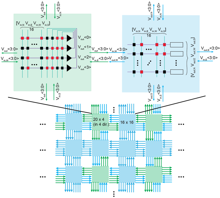
The image depicts a schematic of an interconnected processing array, showcasing the data flow between processing elements. It illustrates the input and output voltage signals (V_in and V_out) for individual processing units and the overall array structure. The diagram highlights the connectivity and data routing within the array.
### Components/Axes
* **Processing Elements (PEs):** The array consists of multiple processing elements arranged in a grid-like structure. Each PE is represented by a square block, colored either light blue or light green.
* **Input Voltage Signals (V_in):** Input voltage signals are labeled as V_in, with directional subscripts (N, E, W, S) indicating the direction from which the signal originates (North, East, West, South). Each V_in signal is a 4-bit vector, denoted by "<3:0>".
* **Output Voltage Signals (V_out):** Output voltage signals are labeled as V_out, with directional subscripts (N, E, W, S) indicating the direction in which the signal is sent. Each V_out signal is a 4-bit vector, denoted by "<3:0>".
* **Internal Structure of PEs:** Two zoomed-in views of the internal structure of the PEs are shown at the top of the diagram. These views illustrate the arrangement of internal components (represented by black and red squares) and the routing of signals within the PE.
* **Array Dimensions:** The array is composed of blocks of "20 x 4 (in 4 dir.)" and "16 x 16" processing elements.
* **Arrows:** Arrows indicate the direction of data flow between processing elements. Blue arrows represent data flow in one direction, while green arrows represent data flow in another direction.
### Detailed Analysis
**Zoomed-In PE Structures:**
* **Left PE Structure:** This structure shows a 4x4 grid of interconnected components. The input signals V_in,N, V_in,E, V_in,W, and V_in,S enter the PE. Red squares are interspersed among black squares. Four output signals, V_out<0>, V_out<1>, V_out<2>, and V_out<3>, are generated by four triangle-shaped components.
* **Right PE Structure:** This structure also shows a grid of interconnected components. The input signals V_in,N, V_in,E, V_in,W, and V_in,S enter the PE. Red squares are interspersed among black squares. The output signals V_out,N, V_out,E, V_out,W, and V_out,S exit the PE.
**Array Interconnection:**
* The processing elements are interconnected in a grid-like fashion.
* Arrows indicate the direction of data flow between adjacent PEs.
* The array appears to be expandable, as indicated by the ellipsis (...) symbols at the edges.
### Key Observations
* The diagram emphasizes the data flow and connectivity within the processing array.
* The use of directional subscripts for V_in and V_out signals indicates a structured data routing scheme.
* The internal structure of the PEs suggests a complex processing capability within each element.
### Interpretation
The diagram illustrates a parallel processing architecture where data is processed and routed between interconnected processing elements. The use of 4-bit voltage signals suggests a digital processing approach. The grid-like arrangement and directional data flow indicate a systolic array-like architecture, where data is pumped through the array in a synchronized manner. The different colors of the processing elements (light blue and light green) might indicate different types of processing units or different states within the array. The diagram provides a high-level overview of the array's structure and data flow, highlighting its potential for parallel processing applications.