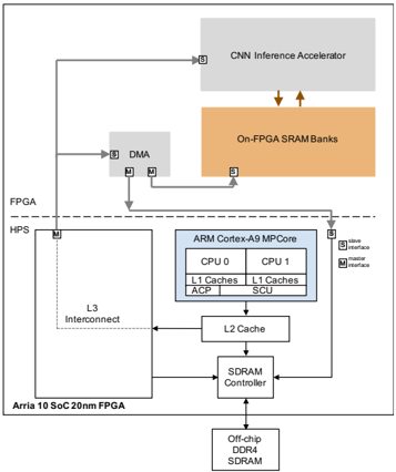
## System Diagram: Arria 10 SoC FPGA Architecture
### Overview
The image is a system diagram illustrating the architecture of an Arria 10 SoC (System on Chip) 20nm FPGA. It depicts the interconnection of various components, including a CNN Inference Accelerator, On-FPGA SRAM Banks, DMA (Direct Memory Access), an ARM Cortex-A9 MPCore, L3 Interconnect, L2 Cache, SDRAM Controller, and Off-chip DDR4 SDRAM. The diagram highlights the data flow and interfaces between these components within the FPGA and HPS (Hard Processor System) domains.
### Components/Axes
* **FPGA:** Field Programmable Gate Array section of the SoC.
* **HPS:** Hard Processor System section of the SoC.
* **CNN Inference Accelerator:** A block for accelerating Convolutional Neural Network inference.
* **On-FPGA SRAM Banks:** On-chip Static Random-Access Memory.
* **DMA:** Direct Memory Access controller.
* **ARM Cortex-A9 MPCore:** A multi-core ARM processor. Contains:
* CPU 0
* CPU 1
* L1 Caches (for both CPUs)
* ACP (Accelerator Coherency Port)
* SCU (Snoop Control Unit)
* **L3 Interconnect:** Interconnect fabric for the HPS.
* **L2 Cache:** Level 2 cache memory.
* **SDRAM Controller:** Controller for external SDRAM.
* **Off-chip DDR4 SDRAM:** External Dynamic Random-Access Memory.
* **Arria 10 SoC 20nm FPGA:** Label for the overall chip.
* **Slave Interface (S):** Denoted by the letter 'S' in a square.
* **Master Interface (M):** Denoted by the letter 'M' in a square.
### Detailed Analysis
* **CNN Inference Accelerator:** Located at the top of the diagram, within the FPGA domain. It has a slave interface.
* **On-FPGA SRAM Banks:** Located below the CNN Inference Accelerator, within the FPGA domain. It has a slave interface. Data flows between the CNN Inference Accelerator and the On-FPGA SRAM Banks, indicated by two downward-pointing arrows.
* **DMA:** Located to the left of the On-FPGA SRAM Banks, within the FPGA domain. It has both slave and master interfaces.
* **FPGA/HPS Boundary:** A dashed line separates the FPGA and HPS domains.
* **ARM Cortex-A9 MPCore:** Located within the HPS domain. It has a slave interface.
* **CPU 0 and CPU 1:** Each CPU has its own L1 Cache.
* **ACP and SCU:** Are also components within the ARM Cortex-A9 MPCore.
* **L3 Interconnect:** Located to the left of the ARM Cortex-A9 MPCore, within the HPS domain. It has a master interface.
* **L2 Cache:** Located below the ARM Cortex-A9 MPCore.
* **SDRAM Controller:** Located below the L2 Cache.
* **Off-chip DDR4 SDRAM:** Located at the bottom of the diagram.
* **Data Flow:**
* The CNN Inference Accelerator connects to the DMA via a line.
* The DMA connects to the On-FPGA SRAM Banks via two lines.
* The L3 Interconnect connects to the SDRAM Controller.
* The L2 Cache connects to the L3 Interconnect and the SDRAM Controller.
* The SDRAM Controller connects to the Off-chip DDR4 SDRAM.
### Key Observations
* The diagram illustrates a typical data processing pipeline, where the CNN Inference Accelerator processes data stored in the On-FPGA SRAM Banks.
* The DMA facilitates data transfer between the CNN Inference Accelerator and the On-FPGA SRAM Banks.
* The ARM Cortex-A9 MPCore interacts with the L2 Cache and SDRAM Controller to access external memory.
* The FPGA and HPS domains are clearly separated, indicating the partitioning of functionality between the programmable logic and the hard processor system.
### Interpretation
The diagram provides a high-level overview of the Arria 10 SoC FPGA architecture, emphasizing the data flow and interconnection of key components. It highlights the integration of a CNN Inference Accelerator, which suggests the device is designed for applications involving machine learning and image processing. The presence of both on-chip SRAM and off-chip DDR4 SDRAM indicates a memory hierarchy optimized for performance and capacity. The separation of the FPGA and HPS domains allows for flexible hardware acceleration and software control. The master and slave interfaces indicate the direction of data flow and control between the different components. Overall, the architecture is designed to support a wide range of embedded applications requiring high performance and low power consumption.