\n
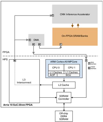
## Diagram: FPGA System Architecture with CNN Inference Accelerator
### Overview
The image depicts a block diagram illustrating the architecture of an FPGA (Field-Programmable Gate Array) system, specifically an Arria 10 SoC 20nm FPGA, integrated with a CNN (Convolutional Neural Network) Inference Accelerator. The diagram showcases the data flow and interconnections between various components, including the FPGA HPS (Hard Processor System), ARM Cortex-A9 MPCore, memory components, and the CNN accelerator.
### Components/Axes
The diagram is composed of several key components:
* **FPGA HPS:** Located on the left side of the diagram, labeled "FPGA HPS".
* **Arria 10 SoC 20nm FPGA:** Located below the "FPGA HPS" label.
* **L3 Interconnect:** Connects the FPGA HPS to other components.
* **ARM Cortex-A9 MPCore:** A dual-core processor with CPU 0 and CPU 1, each having L1 Caches (ACP and SCU).
* **L2 Cache:** Connected to the ARM Cortex-A9 MPCore.
* **SDRAM Controller:** Connected to the L2 Cache.
* **Off-chip DDR4 SDRAM:** Memory connected to the SDRAM Controller.
* **DMA:** Direct Memory Access controller.
* **CNN Inference Accelerator:** Located at the top of the diagram.
* **On-FPGA SRAM Banks:** Memory connected to the CNN Inference Accelerator.
* **Interfaces:** Marked with "M" (Master) and "S" (Slave) labels, indicating the interface type.
* **Data Flow Arrows:** Indicate the direction of data transfer between components.
### Detailed Analysis or Content Details
The diagram illustrates the following data flow:
1. Data flows from the FPGA HPS through the L3 Interconnect to the ARM Cortex-A9 MPCore.
2. Within the ARM Cortex-A9 MPCore, data is processed by CPU 0 and CPU 1, utilizing their respective L1 Caches (ACP and SCU).
3. Data is then passed to the L2 Cache and subsequently to the SDRAM Controller.
4. The SDRAM Controller manages access to the Off-chip DDR4 SDRAM.
5. Data also flows from the FPGA HPS to the DMA controller.
6. The DMA controller transfers data to the CNN Inference Accelerator.
7. The CNN Inference Accelerator utilizes On-FPGA SRAM Banks for data storage and processing.
8. The CNN Inference Accelerator has a slave interface to the ARM Cortex-A9 MPCore.
9. The FPGA HPS has a master interface to the ARM Cortex-A9 MPCore.
The interfaces are labeled as follows:
* The connection between the FPGA HPS and the ARM Cortex-A9 MPCore is labeled with both "M" (Master) and "S" (Slave) interfaces.
* The connection between the CNN Inference Accelerator and the ARM Cortex-A9 MPCore is labeled with a "S" (Slave) interface.
* The connection between the DMA and the FPGA HPS is labeled with "M" (Master) and "S" (Slave) interfaces.
### Key Observations
The diagram highlights the integration of a dedicated CNN Inference Accelerator within an FPGA system. This suggests an architecture optimized for accelerating CNN-based applications. The use of both on-chip (SRAM Banks) and off-chip (DDR4 SDRAM) memory indicates a hierarchical memory system designed to balance speed and capacity. The presence of DMA suggests efficient data transfer mechanisms. The dual-core ARM processor provides general-purpose processing capabilities alongside the specialized CNN accelerator.
### Interpretation
This diagram represents a heterogeneous computing architecture. The FPGA provides a flexible platform for implementing custom hardware accelerators like the CNN Inference Accelerator. The ARM Cortex-A9 MPCore handles control and general-purpose tasks, while the CNN accelerator offloads computationally intensive CNN operations. The DMA controller facilitates efficient data transfer between the FPGA HPS, the CNN accelerator, and the memory system. The architecture is designed to achieve high performance and energy efficiency for CNN-based applications by leveraging the strengths of both hardware and software components. The use of both on-FPGA SRAM and off-chip DDR4 SDRAM suggests a strategy to optimize memory access patterns for the CNN accelerator, utilizing fast on-chip memory for frequently accessed data and larger off-chip memory for storing the entire model and datasets. The master/slave interface designations indicate the control flow and data access permissions between the different components. The diagram suggests a system where the FPGA HPS initiates data transfers and controls the overall operation, while the CNN accelerator operates as a co-processor.