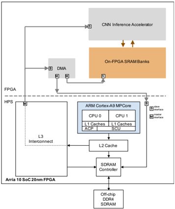
## Diagram: CNN Inference Accelerator Architecture
### Overview
The diagram illustrates a heterogeneous computing system architecture for CNN inference acceleration. It integrates FPGA, ARM Cortex-A9 MPCore, DDR4 SDRAM, and On-FPGA SRAM Banks, with data flow managed via L3 Interconnect, DMA, and master/slave interfaces.
### Components/Axes
- **Key Components**:
- **FPGA**: Arria 10 SoC 20nm FPGA (left side).
- **HPS**: Connected to FPGA via L3 Interconnect.
- **ARM Cortex-A9 MPCore**: Central block with dual CPUs (CPU0, CPU1), L1/L2 caches, ACP, SCU, and SDRAM Controller.
- **Off-chip DDR4 SDRAM**: Connected to SDRAM Controller.
- **CNN Inference Accelerator**: Top-right block, linked to On-FPGA SRAM Banks.
- **On-FPGA SRAM Banks**: Orange block, directly connected to CNN Inference Accelerator.
- **DMA**: Gray block, bridges FPGA and ARM Cortex-A9 MPCore.
- **Data Flow**:
- Arrows indicate bidirectional communication (e.g., FPGA ↔ HPS, ARM ↔ DDR4 SDRAM).
- Master/slave interfaces (labeled "M" and "S") define communication roles.
### Detailed Analysis
- **FPGA and HPS**:
- FPGA (Arria 10 SoC 20nm) connects to HPS via L3 Interconnect.
- DMA mediates data transfer between FPGA and ARM Cortex-A9 MPCore.
- **ARM Cortex-A9 MPCore**:
- Dual CPUs (CPU0, CPU1) with shared L1 caches.
- ACP (Advanced Communication Peripheral) and SCU (System Control Unit) manage system-level tasks.
- L2 Cache sits between CPUs and SDRAM Controller.
- **Memory Hierarchy**:
- Off-chip DDR4 SDRAM is the primary memory, controlled by the SDRAM Controller.
- On-FPGA SRAM Banks provide low-latency access for the CNN Inference Accelerator.
- **CNN Inference Accelerator**:
- Directly connected to On-FPGA SRAM Banks, suggesting optimized data throughput for inference tasks.
### Key Observations
1. **Hierarchical Design**:
- FPGA and HPS handle peripheral/data acquisition, while ARM Cortex-A9 MPCore manages general computation.
- CNN Inference Accelerator offloads specialized tasks to On-FPGA SRAM for speed.
2. **Memory Optimization**:
- On-FPGA SRAM Banks reduce latency for the CNN accelerator compared to off-chip DDR4 SDRAM.
- L3 Interconnect and DMA enable efficient data sharing between FPGA and ARM cores.
3. **Interface Roles**:
- Master/slave labels ("M" and "S") clarify communication directionality (e.g., FPGA as master to HPS).
### Interpretation
This architecture prioritizes **performance isolation** and **data locality**:
- The CNN Inference Accelerator leverages On-FPGA SRAM for rapid access, critical for low-latency inference.
- ARM Cortex-A9 MPCore handles general-purpose tasks, offloading compute-heavy CNN work to the FPGA.
- The use of DMA and L3 Interconnect minimizes CPU overhead for data transfers, improving scalability.
The design reflects a **coarse-grained parallelism** approach, where specialized hardware (FPGA accelerator) and general-purpose cores (ARM) collaborate via optimized memory and interconnects. The absence of explicit numerical values suggests a focus on architectural relationships rather than quantitative benchmarks.