## Diagram: AIMC Training and Inference with ReRAM-based AI Core
### Overview
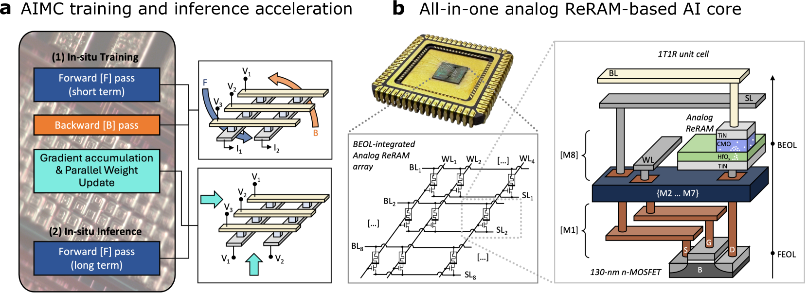
The image presents a diagram illustrating the acceleration of AI model training and inference using an Analog In-Memory Computing (AIMC) architecture. It highlights the in-situ training and inference processes, along with a detailed view of an all-in-one analog ReRAM-based AI core. The diagram is divided into two main sections: (a) AIMC training and inference acceleration, and (b) All-in-one analog ReRAM-based AI core.
### Components/Axes
**Section a: AIMC training and inference acceleration**
* **(1) In-situ Training:**
* **Forward [F] pass (short term):** Represented by a blue box.
* **Backward [B] pass:** Represented by an orange box.
* **Gradient accumulation & Parallel Weight Update:** Represented by a cyan box.
* **(2) In-situ Inference:**
* **Forward [F] pass (long term):** Represented by a blue box.
* **Diagrams:**
* Top diagram shows the forward pass (F) and backward pass (B) with voltages V1, V2, V3 and currents I1, I2.
* Bottom diagram shows the forward pass with voltages V1, V2, V3.
**Section b: All-in-one analog ReRAM-based AI core**
* **Top-right:** 1T1R unit cell
* BL (Bit Line)
* SL (Source Line)
* Analog ReRAM stack:
* TIN (Titanium Nitride)
* CMO (Conductive Metal Oxide)
* HfOₓ (Hafnium Oxide)
* TIN (Titanium Nitride)
* WL (Word Line)
* {M2 ... M7}
* [M8]
* [M1]
* 130-nm n-MOSFET
* S (Source)
* G (Gate)
* D (Drain)
* B (Body)
* BEOL (Back-End-Of-Line)
* FEOL (Front-End-Of-Line)
* **Bottom-left:** BEOL-integrated Analog ReRAM array
* BL1, BL2, BL8 (Bit Lines)
* WL1, WL2, WL4 (Word Lines)
* SL1, SL2, SL8 (Source Lines)
### Detailed Analysis or ### Content Details
**Section a: AIMC training and inference acceleration**
* The diagram illustrates the flow of data and operations during in-situ training and inference.
* The forward pass is used in both training (short term) and inference (long term).
* The backward pass and gradient accumulation are specific to the training phase.
* The arrows indicate the direction of data flow and the sequence of operations.
**Section b: All-in-one analog ReRAM-based AI core**
* The diagram shows a chip package with the ReRAM-based AI core.
* The ReRAM array is organized in a grid with bit lines (BL), word lines (WL), and source lines (SL).
* The 1T1R unit cell consists of a transistor and a ReRAM element.
* The ReRAM element is composed of TIN, CMO, and HfOₓ layers.
* The diagram highlights the BEOL and FEOL layers in the device.
* The 130-nm n-MOSFET is used as the access transistor for the ReRAM cell.
### Key Observations
* The AIMC architecture integrates training and inference on the same chip.
* The ReRAM-based AI core enables analog in-memory computing.
* The 1T1R unit cell is a fundamental building block of the ReRAM array.
* The diagram provides a detailed view of the device structure and components.
### Interpretation
The diagram illustrates a novel approach to AI acceleration using analog in-memory computing with ReRAM technology. By performing computations directly within the memory array, the AIMC architecture can potentially reduce energy consumption and improve performance compared to traditional digital computing architectures. The integration of training and inference on the same chip enables efficient on-device learning and adaptation. The detailed view of the ReRAM cell and array provides insights into the device structure and operation. The use of HfOₓ as the resistive switching material is a common choice in ReRAM devices due to its good performance and reliability. The 130-nm n-MOSFET provides the necessary switching functionality for accessing and controlling the ReRAM cell. Overall, the diagram highlights the potential of ReRAM-based AIMC for enabling energy-efficient and high-performance AI applications.