\n
## Diagram: AIMC Training and Inference Acceleration & All-in-one Analog ReRAM-based AI Core
### Overview
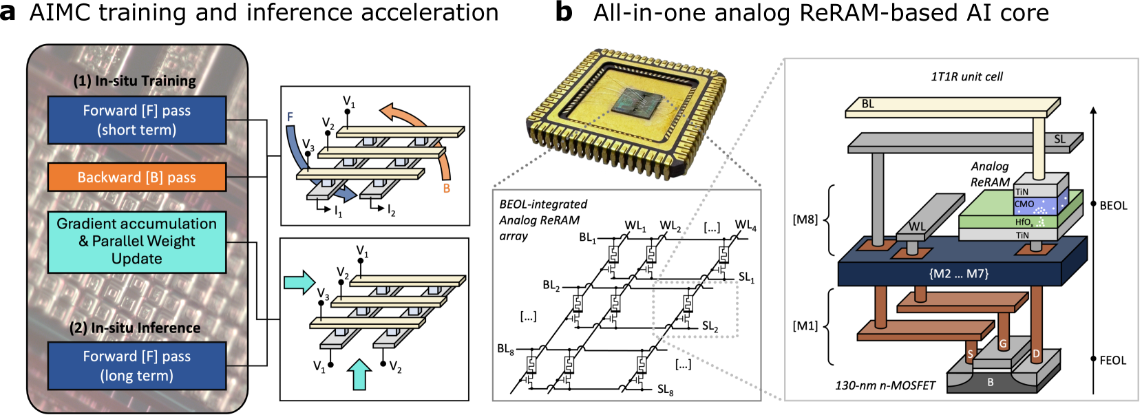
The image presents a diagram illustrating the architecture and process flow for AIMC (Analog In-Memory Computing) training and inference acceleration using an all-in-one analog ReRAM-based AI core. It is divided into two main sections: (a) depicting the training and inference process, and (b) detailing the core's structure.
### Components/Axes
Section (a) shows a flow diagram with labeled blocks representing stages of the process. Section (b) displays a schematic of the ReRAM array and a 3D representation of a single ReRAM unit cell. Key labels include: "Forward (F) pass (short term)", "Backward (B) pass", "Gradient accumulation & Parallel Weight Update", "Forward (F) pass (long term)", "BEOL-integrated Analog ReRAM array", "1T1R unit cell", "Analog ReRAM", "BEOL", "FEOL", "130-nm n-MOSFET", "WL1…WL4", "BL1…BL8", "SL1…SL4", "WL", "BL", "SL", "Tin", "CMO", "HfO2", "G", "B", "S", "I1", "I2", "V1", "V2", "V3".
### Detailed Analysis or Content Details
**Section (a): AIMC Training and Inference Acceleration**
This section illustrates a process flow.
1. **In-situ Training:** This block is divided into two sub-processes:
* **Forward (F) pass (short term):** Depicted with a schematic showing a ReRAM device with input voltages V1 and V2, and output currents I1 and I2. Arrows indicate the flow of current.
* **Backward (B) pass:** Also depicted with a ReRAM device schematic, similar to the forward pass.
2. **Gradient accumulation & Parallel Weight Update:** A rectangular block connecting the training stages.
3. **In-situ Inference:** This block is divided into:
* **Forward (F) pass (long term):** Depicted with a ReRAM device schematic, similar to the forward pass.
**Section (b): All-in-one Analog ReRAM-based AI Core**
This section shows the physical structure of the core.
1. **BEOL-integrated Analog ReRAM array:** A schematic representation of a ReRAM array with multiple word lines (WL1-WL4) and bit lines (BL1-BL8), connected to source lines (SL1-SL4). The array is represented as a grid of cells.
2. **1T1R unit cell:** A 3D representation of a single ReRAM unit cell. The cell consists of:
* **Analog ReRAM:** Layered structure with Tin, CMO, and HfO2 materials.
* **BEOL (Back End of Line):** Indicated as a layer above the ReRAM.
* **FEOL (Front End of Line):** Indicated as a layer below the ReRAM, containing a 130-nm n-MOSFET with gate (G), body (B), and source/drain (S) terminals.
* **M1-M8:** Representing metal layers.
### Key Observations
The diagram highlights the integration of ReRAM devices with standard CMOS technology. The ReRAM array is positioned on top of the MOSFETs, indicating a 3D integration scheme. The training process involves both forward and backward passes, suggesting an in-memory learning approach. The use of analog computation is emphasized by the "Analog ReRAM" label.
### Interpretation
The diagram demonstrates a novel architecture for AI acceleration that leverages the benefits of both analog computation and in-memory processing. By integrating ReRAM devices directly with CMOS circuitry, the design aims to reduce data movement and energy consumption, which are major bottlenecks in traditional AI systems. The in-situ training capability suggests that the system can adapt and learn directly within the memory array, eliminating the need for frequent data transfers to and from the processor. The layered structure of the ReRAM cell (Tin, CMO, HfO2) indicates the materials used to achieve the desired resistive switching characteristics. The diagram suggests a potential pathway for building more efficient and powerful AI hardware. The use of BEOL integration is a key feature, allowing for high-density ReRAM arrays without impacting the performance of the underlying CMOS transistors.